Nantero Exits Stealth: Using Carbon Nanotubes for Non-Volatile Memory with DRAM Performance & Unlimited Endurance
by Kristian Vättö on June 11, 2015 12:35 PM EST- Posted in
- Storage
- DRAM
- Semiconductors
- Nantero
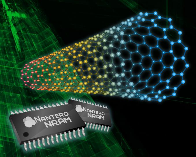
- NRAM
The race for next generation non-volatile memory technology is already on at full throttle. We covered Crossbar’s ReRAM announcement last year and last week a very exciting company with a different non-volatile technology exited stealth mode and shed light on its technology and commercialization plans. The company is called Nantero and it’s been developing its NRAM technology for well over a decade now.

Before we talk about the technology itself, let’s briefly discuss the company and its key persons as Nantero is probably an unfamiliar name to many (it was for me, at least). The company was founded by Greg Schmergel, Dr. Tom Rueckes and Dr. Brent M. Segal in 2001. Mr. Schmergel and Dr. Rueckes are both still with the company and serve as CEO and CTO respectively, but Dr. Segal left the company in 2008 as a part of Nantero's Government Business Unit acquisition by Lockheed Martin. Mr. Schmergel is a well renowned serial entrepreneur who founded ExpertCentral that was later acquired by About.com where Mr. Schmergel served as a Senior Vice President before co-founding Nantero. While Mr. Schmergel brings valuable business expertise to the company, the technology comes from Dr. Tom Rueckes who is a Harvard Ph.D in chemistry and the inventor of NRAM technology.
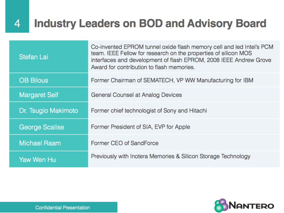
The Board of Directors includes several semiconductor industry veterans. Mr. Lai was one of the leading developers of NAND technology at Intel and also led Intel’s Phase Change Memory (PCM) team. Dr. Makimoto is a former Chief Technologist of Sony and Hitachi and Mr. Scalise is actually the former President of Silicon Industry Association (SIA) and also served as an Executive Vice President at Apple briefly in the late 90s. Mr. Raam may too be a familiar name to some since he is the former CEO of SandForce (the SSD controller company) that is now owned by Seagate.
The Technology
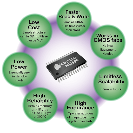
It goes without saying that Nantero is packed with semiconductor experience and know-how, but its technology isn’t any less interesting. NRAM is made out of carbon nanotubes, which is the strongest material known to man and provides far better thermal and electrical conductivity than any other known material.
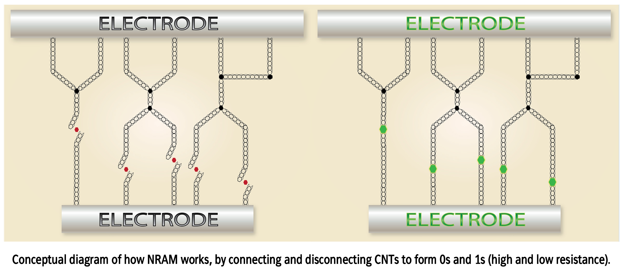
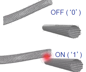
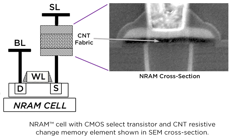
The way NRAM works is in fact relatively simple. Essentially there are two nanotubes, which have low resistance when in physical contact and high resistance when separated. The amount of resistance then determines whether the cell is considered to be programmed as ‘0’ or ‘1’. Program operation (or “SET” as Nantero calls it) works by applying a voltage on one of the nanotubes, which will then attract the other nanotube and create a bond. The SET operation is very fast and takes only picoseconds, which is on par with or better than DRAM latency. The bond is kept in tact by Van der Waal's interactions and is practically immortal with data retention terms even in 300°C is over ten years. In an erase operation (or RESET as Nantero calls it) the voltage is simply applied in the other direction, which will “heat up” (given the scale it’s more like vibration) the nanotube contacts and cause them to separate. Given that carbon nanotubes are one of the strongest materials in the world, the write/erase endurance is practically infinite as independent university study has shown Nantero’s NRAM technology to have over 1011 P/E cycles (for your information, 1011 translates to 100 billion).
The other great news is that carbon nanotubes are extremely small. One nanotube can have a diameter of only 2nm and the pitch between the two nanotubes in off-state can be an even tinier 1nm, so the technology has potential to scale below 5nm. NRAM can also scale vertically, or go 3D, and since the cell structure and manufacturing process are both quite simple, 3D stacking should, in theory, be much easier compared to what 3D NAND is today with no need for high aspect ratio etching as an example.
The Manufacturing Process
The process of making an NRAM wafer starts by taking a normal CMOS wafer with the normal cell select and array line circuitry, which is then spin coated with carbon nanotubes. Carbon nanotubes are grown from iron that would normally contaminate a clean room, thus Nantero had to develop a patented process that creates ‘pure’ carbon nanotubes with less than one out of billion particles being foreign (the standard for the highest quality clean rooms). Nantero has worked hard in the past two years to bring the cost of carbon nanotubes down and currently the company says that the nanotubes have a negligible impact on chip cost, meaning making NRAM isn't inherently more expensive than any other semiconductor.
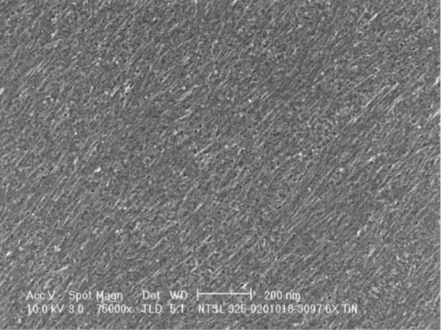
Top-down SEM of NRAM
With the nanotubes on the wafer, the top electrode is deposited on top of the nanotubes, followed by the photoresist, which is then patterned using a single mask. Finally the wafer is etched to cut the nanotubes into smaller pieces (i.e. more memory cells) and that’s it in a nutshell. Obviously there are other general semiconductor processing steps involved, but those are the same for all memory technologies, so the fundamental process of manufacturing NRAM isn’t that complex. All that is needed is a normal CMOS fab because the NRAM process requires no special or additional tools.
Fortunately, NRAM isn’t just a technology that exists on paper. Nantero’s NRAM process has already been installed in seven production CMOS fabs ranging from 20nm to 250nm and limited production has been taking place for several years now, although only in small few megabit capacities. As a matter of fact, Nantero completed a successful space test with NASA on Space Shuttle Atlantis back in 2009 where NRAM operated without any shielding throughout the trip without any errors despite the intense radiation, because as I mentioned earlier, the nanotube bonds are practically unbreakable and are not affected by heat, magnetism, radiation and the like.
Nantero’s Business Plan: Bringing NRAM to Everyone
Because Nantero is an IP licensing company, it relies solely on its partners for production. It's a logical strategy because a decent sized fab requires an investment in the order of billions of dollars and in the end the company would have to compete against Intel, Samsung and the rest of the semiconductor giants. Actual end products will be sold under the manufacturer's brand (e.g. Intel), so you won't see any Nantero branded products on the market.
Nantero isn't disclosing any of its partners at this point as most of them are still developing products that have the potential for higher volume production. While Nantero has its own chip team that is developing high capacity (several gigabits) dies, every partner is also doing its own work to implement NRAM at a larger scale, which makes sense given that the big semiconductor companies have far more resources and are familiar with high capacity memory devices.
Aside from semiconductor companies, Nantero has also partnered with several more consumer-facing companies to develop concepts and products around NRAM technology. Since NRAM provides the same level of performance as DRAM but is non-volatile, NRAM could open the doors for products that aren't achievable (at least properly) with today's NAND and DRAM technology. As examples Nantero mentions 3D smartphones and commercial 3D printers (although to be frank both already exist to some extent), but practically anything that's handicapped by IO performance and volatility can be fixed with NRAM in the future.
Since it will take several years before NRAM is even close to modern NAND capacities, Nantero has a three step strategy of bringing NRAM to the market. In the first step Nantero is simply offering a class of memory (both standalone and embedded) that has DRAM's performance characteristics and NAND's non-volatility. Technically that means NRAM is competing against current MRAM and ReRAM products for a specialized niche market that really needs high performance and non-volatility. The consumer market is obviously not one of those and even for the enterprise NRAM is likely too small capacity and expensive, but the industrial and especially space/military applications should benefit from NRAM despite the high initial cost.
The next step is to grow NRAM to gigabit-class capacities and offer a non-volatile alternative to DRAM. Going to gigabit-class certainly opens the doors for NRAM as a mainstream memory because it could be used for a variety of caching applications that benefit from non-volatility (SSDs with their DRAM caches for NAND mapping table are a prime example). Tape out of first gigabit NRAM wafers is still about 18 months away, so I would expect to see something shipping perhaps in late 2017 or 2018.
The final step, of course, is a terabit-class die to replace NAND (FYI, Samsung is projecting 1Tbit NAND die in 2017). Achieving that requires work on both lithography scaling and 3D integration technologies because such a high capacity die is only economical with either multiple layers or advanced lithography, or both.
NRAM also has the potential to operate in MLC mode for further density improvements, but for now Nantero is focusing on scaling NRAM down and adding layers through 3D to increase density. Once the work on those two is done and has been implemented to a production fab, Nantero will start commercializing NRAM MLC technology, but that is likely at least several years away.
Final Words
The announcement is intriguing to say the least. From a technology standpoint NRAM sounds very exciting because it's effectively bringing us non-volatile DRAM performance, and better yet the cell design is scalable whereas DRAM has major struggles going below 20nm. I like the fact that Nantero has decided to go with IP licensing model because it means that NRAM is a technology available to everyone. The reason why DRAM and NAND are where they are today is because there are multiple companies producing them, resulting in competition with billions of R&D dollars.
I wonder if any of the big semiconductor companies has partnered with Nantero yet. Most of them have been tight-lipped about their post-NAND plans, but maybe Nantero's announcement will sooner than later force the companies to talk about their strategies. Obviously a lot depends on how far 3D NAND can efficiently scale, but from what I have heard the transition to next generation memory technologies should begin around 2020. The future of memory isn't here yet, but it's certainly getting closer and it will be interesting to see what technology ends up taking the crown.


35 Comments
View All Comments
name99 - Friday, June 12, 2015 - link
Hp has given up on this with The Machine. In that the first version of The Machine that ship (if ever) will not have HW unified storage and RAM. They may still be going for a single level store at the SW level (like AS/400 aka iSeries) though that's a harder part of the problem than the HW, and not obviously useful in modern SW contexts.http://www.moorinsightsstrategy.com/the-machine-th...
I don't know enough about this space to understand any more what they are going for in this computer and what the target market is. It seems to be heading towards a box with an insane amount of memory in it and some number of smallish cores --- so memcached type servers? (not much money in that) and all-RAM super-huge Oracle databases? (lotsa money in that)
Jaybus - Tuesday, June 16, 2015 - link
Most processors are modified Harvard architecture, since they have a separate L1 instruction cache. Disk (SSD) storage is an i/o operation. NRAM, ReRAM, etc. doesn't change the architecture, but rather eliminates the need for i/o to/from permanent storage. Although, ReRAM also has application in neuromorphic architectures that truly are a paradigm shift.BrokenCrayons - Friday, June 12, 2015 - link
If NRAM is non-volatile and as fast as volatile memory we use today plus has infinite P/E cycles, does that mean there are implications of say, merging our present day SSD/HDD storage and RAM into a single memory repository? That'd simplify system design, improve integration, and reduce PCB space requirements/wiring complexity. It could drive costs lower and (just a total knee-jerk thought based on how each on/off state is made) lower power consumption. I might be having a ditzy moment, but is that possible? It'd be exciting if that was the case.lorribot - Friday, June 12, 2015 - link
Seems to me first use of this would be to replace battery backed write caches in the enterprise. Followed closely by disk write caches on high end NAND based storage, particularly those that have low P/E cycles.Alternative would be an intermediate memory to enable near instantaneous shutdown and boot up to replace standby using hibernation like methodologies.
My only worry is whether hardware and OS support for all this will mean it takes an age for it to become available outside of proprietary/enterprise systems in a reasonable time frame.
I offer NVMe and Thunderbolt as technologies whose widespread adoption that have been painful to watch.
IlllI - Tuesday, June 23, 2015 - link
I can't get past the stupid name for the product. Really? that the best name they could come up with? sound like some comic book villian's name.