The Kaveri Refresh 'Godavari' Review: Testing AMD's A10-7870K
by Ian Cutress on June 1, 2015 11:59 AM EST
Astute readers will recognize that we recently posted two reviews covering more of the stack of AMD processors with the codename 'Kaveri' which covered the A6-7400K, A8-7650K and the A10-7700K in our recent coverage. Today we review the newest element that sits on top of all others, the A10-7870K Kaveri Refresh APU.
What's in a name?
Rumors regarding an update to AMDs APU line have been permeating through the technology media for some weeks. Some seemed true, others obviously false and almost all posted without verification (which is the point where we at AT would post). However all of them revolved around the notion that AMD needed to update Kaveri, and perhaps pointing fingers at the new Excavator cores in the laptop focused Carrizo would be part of the line.
The A10-7870K is not a permutation of Carrizo. It relies on the same Steamroller cores as Kaveri, hence the title 'Kaveri Refresh', and has the same underlying architecture as Kaveri.
Ultimately the A10-7870K is the same core and same architecture underneath, but with a few added benefits detailed below. When it comes to naming, a number of sites and publications within the media have called the new line ‘Godavari’, and where the name Godavari comes in to all this is down to AMD's internal codenames rather than anything put forward by marketing. We were told that any slides published with that name are usually aimed for internal AMD or B2B use, but that also the ‘Kaveri Refresh’ indication was again, an internal codename. One could argue the merits in using either codename, and I’m sure the ‘Godavari’ moniker will run riot, although I think Kaveri Refresh more accurately describes the new APU launch and subsequent models to follow.
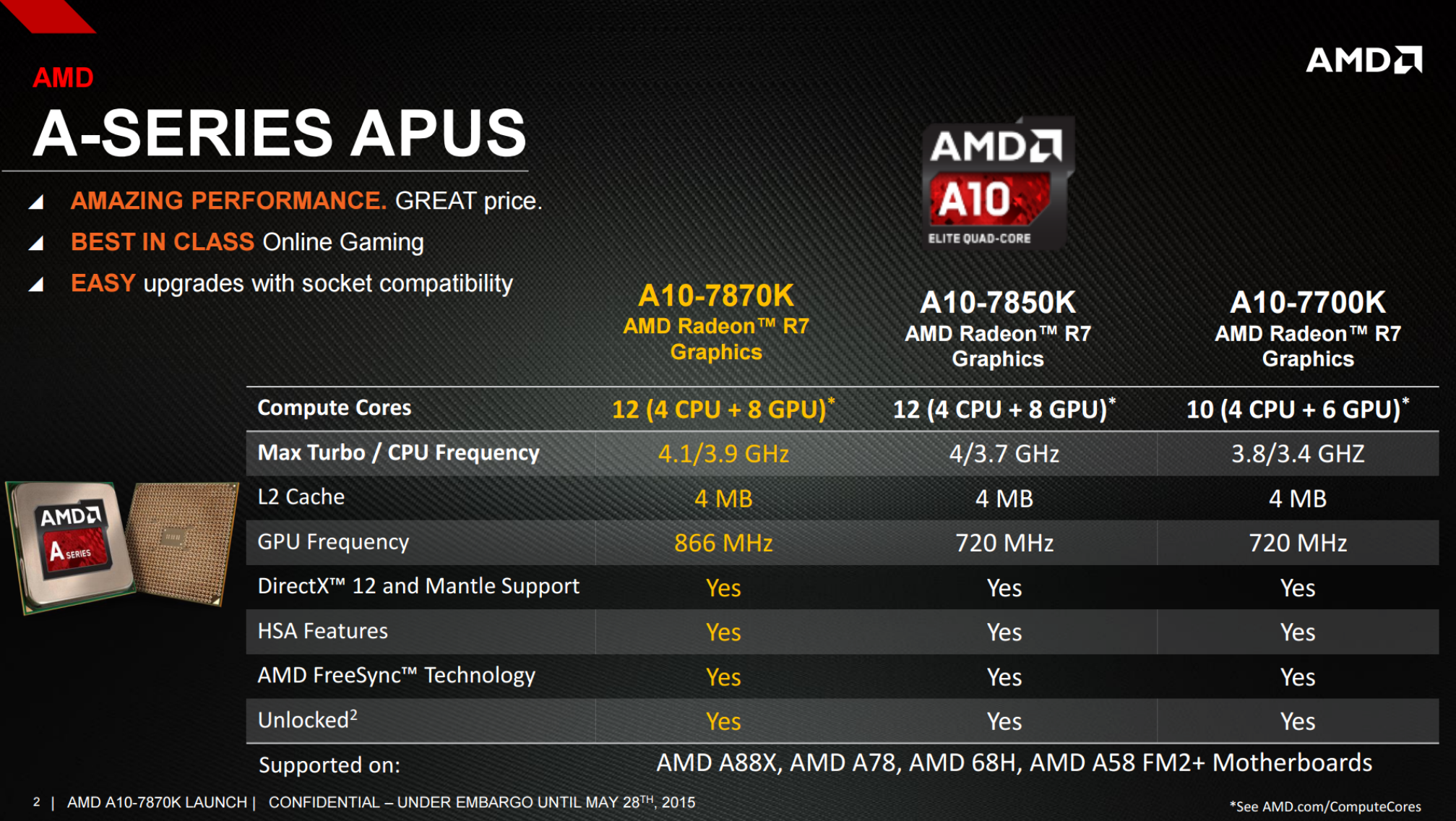
AMD is launching one consumer APU to begin with, with more (both consumer and commercial) to follow in the coming weeks and months. The purpose of the A10-7870K is to show that AMD is working at improving the silicon process and is able to achieve more with the same. The home hitting statistic from the new APU is a jump in clock speeds compared to the previous king of APUs, the A10-7850K.
| AMD Kaveri Lineup | ||||||||
| A10- 7870K |
A10- 7850K |
A10- 7800 |
A10- 7700K |
A8- 7650K |
A8- 7600 |
X4 860K |
A6- 7400K |
|
| Price | $137 | $134 | $131 | $120 | $104 | $89 | $85 | $64 |
| Modules | 2 | 2 | 2 | 2 | 2 | 2 | 2 | 1 |
| Threads | 4 | 4 | 4 | 4 | 4 | 4 | 4 | 2 |
| Core Freq. (GHz) | 3.9-4.1 | 3.7-4.0 | 3.5-3.9 | 3.4-3.8 | 3.3-3.8 | 3.1-3.8 | 3.7-4.0 | 3.5-3.9 |
| Compute Units | 4+8 | 4+8 | 4+8 | 4+6 | 4+6 | 4+6 | 4+0 | 2+4 |
| Streaming Processors |
512 | 512 | 512 | 384 | 384 | 384 | N/A | 256 |
| IGP Freq. (MHz) | 866 | 720 | 720 | 720 | 720 | 720 | N/A | 756 |
| TDP | 95W | 95W | 65W | 95W | 95W | 65W | 95W | 65W |
| DRAM Frequency |
2133 | 2133 | 2133 | 2133 | 2133 | 2133 | 1866 | 1866 |
| L2 Cache | 2x2MB | 2x2MB | 2x2MB | 2x2MB | 2x2MB | 2x2MB | 2x2MB | 1MB |
The bottom line is a bump in base frequency to 3.9GHz and turbo frequency to 4.1GHz giving more grunt in common tasks. The bigger jump, and arguable the more important, is the integrated graphics. We move from 720 MHz to 866 MHz, a boost of 20% on the 512SP core. With AMDs heterogeneous system architecture approach on the APU line, this is arguably the best place to put any potential increases due to process improvements and better binning. When speaking to AMD, it transpires that this boost on the Kaveri design is due to three things: an improved process, binning, and a marginal voltage increase (which is doubly effective due to the binning). The stock voltage of the processor goes up 0.050 volts compared to the 7850K, although AMD still reports a 95W TDP. Usually stock voltages are listed as a range depending on the quality of the die, but on average that window is slightly higher this time around. But as the TDP is similar, this ultimately should not matter that much. We have our power testing later in this review.
Going back to the A10-7850K, at launch it was listed as $172, designed to compete with Intel but provide better integrated graphics (or APU + dGPU combo) for the similar budget. The price of the 7850K has come down since then, and currently resides at $135. As a result, the release price of the A10-7870K is suited to this new scale, and we should see it on the shelves for $143. If we compare that directly to an Intel part, we come up against the i3-4360 or i5-4570:
| CPU/APU Comparion | ||||
| AMD Kaveri | Amazon Price on 5/27 |
Intel Haswell | ||
| $236 |
i5-4690K (4C/4T, 88W) |
3.5-3.9 GHz HD 4600 |
||
| $214 | i5-4590 (4C/4T, 84W) |
3.3-3.7 GHz HD 4600 |
||
| $189 | i5-4460 (4C/4T, 84W) |
3.2-3.4 GHz HD 4600 |
||
| 3.9-4.1 GHz 512 SPs |
A10-7870K (2C/4T, 95W) |
$137 / $138 | i3-4330 (2C/4T, 54W) |
3.5 GHz HD 4600 |
| 3.7-4.0 GHz 512 SPs |
A10-7850K (2M/4T, 95W) |
$134 | ||
| 3.5-3.9 GHz 512 SPs |
A10-7800 (2M/4T, 65W) |
$131 | ||
| 3.4-3.8 GHz 384 SPs |
A10-7700K (2M/4T, 95W) |
$120 | i3-4130 (2C/4T, 54W) |
3.4 GHz HD 4400 |
| 3.3-3.8 GHz 384 SPs |
A8-7650K (2M/4T, 95W) |
$104 | ||
| $94 | Pentium G3430 (2C/2T, 53W) |
3.3 GHz HD (Haswell) |
||
| 3.1-3.8 GHz 384 SPs |
A8-7600 (2M/4T, 65W) |
$89 | ||
| 3.7-4.0 GHz No IGP |
X4 860K (2M/4T, 95W) |
$85 | ||
| $70 | Pentium G3258 (2C/2T, 53W) |
3.2 GHz HD (Haswell) |
||
| 3.5-3.9 GHz 256 SPs |
A6-7400K (1M/2T, 65W) |
$64 | ||
| $44 | Celeron G1840 (2C/2T, 53W) |
2.8 GHz HD (Haswell) |
||
Our previous benchmark numbers show that in pure CPU workloads, AMDs architecture has a tough time in single threaded loads that do not rely on memory. Multithreaded loads also seem to take advantage of the hyperthreads of Intel better than the core design of the Bulldozer base architecture, although some benchmarks and workloads (particularly those that can be accelerated with the internal graphics) favor AMD. Where AMD pulls ahead is typically on the graphics side with the integrated solution of 512 SPs getting better frame rates in both regular and high end titles against a 24/20 execution unit Intel variant. Based on paper alone, the 20% boost in frequency to the 7870K would further cement that lead. However 20% clock speed does not guarantee 20% more performance, especially as top titles are becoming more multithreaded and/or memory bandwidth intensive.
Perhaps because of this, it is worth noting that AMD’s sampling strategy for the A10-7870K was oriented more towards the gaming press than the technology press this time around, and as a result many of the tech websites had to find other sampling sources. AMD’s slides on the Kaveri Refresh launch were, as expected, oriented towards some of the more e-Sports titles currently harvesting millions of players worldwide:
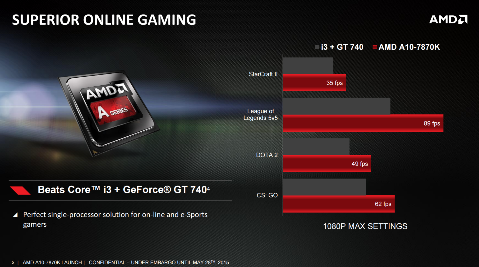
AMD’s strategy at this point is simply that discrete cards go after AAA titles while the APU line grapples with games appealing to a more mass market, or mass audience. The key line in the promotional material we received was all about how an inexpensive system can tackle the common adversarial titles of the generation.
Not to focus all on the eSports titles, we did get a small glimpse into dual graphics compatibility:
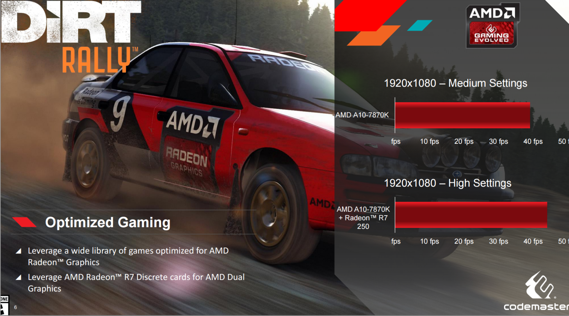
AMD reported a 25% increase in frame rates even when moving from medium to high quality with DIRT Rally when enabling an R7 250 card into the mix for dual graphics. We’ve tested dual graphics in this review as well, with titles like GRID Autosport, to find the parallels and verification for this. Because it’s a question that comes up with almost every APU review, we asked for clarification on dual graphics compatibility with the A10 line of APUs. The results are:
Suggested: A10 APU + R7 250 DDR3
Also works: A10 APU + R7 250 GDDR3 / R7 240 DDR3 / R7 240 GDDR3
AMD suggests DDR3 cards over GDDR3 cards purely to keep memory types similar, although at some point it would be interesting to see the comparison between the different types. For our testing we are using the R7 240 DDR3 model from ASUS, a small $70 discrete card.
Another element AMD is promoting with the Kaveri Refresh line is an upcoming feature in DirectX 12: Multiadapter Rendering / Asymmetric Rendering. DirectX 11 only allows single threaded operation by default with alternate frame rendering, by comparison. The principle behind asymmetric rendering means that each graphics adapter in the system can be identified by its speed and capabilities and assigned an appropriate identifier. Then, at the engine level of the game (making this feature title dependent, not driver dependent) batches of work can be dispatched according to priority, complexity and required efficiency to each of the rendering capable devices in the system. The results are collated into the graphics output.

The example we were given (which I have seen in the flesh) is with the Oxide Games/Stardock upcoming title Ashes of the Singularity. I spoke extensively to Dan Baker of Oxide Games and he states that the concept is relatively simple making it easier for programmers to dive in, and implementing it into their engine for the game took some time but they found a substantial benefit. Ashes of the Singularity is designed to be a more classical type of RTS based in the future, with plenty of units on hand as well as scenery and effects needing to be rendered. In the screenshot above, the red and blue colored items represent the different items that are rendered and the color shows which graphics in the system supplied the processing power. In this case the APU took care of the red units, while the discrete GPU did the scenery and a good portion of the effects. In the demo I was at, enabling the APU in this circumstance gave a 10% performance increase in a heavy 30 FPS scene to 33 FPS. It doesn’t sound like much, but any opportunity to use more of the system that the user has paid for is always a bonus. I asked regarding multiple discrete cards, such as dual R9 290Xs, and he said it wasn’t a problem by the way they had built their engine.
While we do not have access to DX12 and Asymmetric Rendering capable titles as of yet, we are hoping to work closely with developers like Oxide in order to test the main public releases under the new feature sets. Stay tuned.
A new feature coming to the APU line, present on the high end graphics cards, is Virtual Screen Resolution.
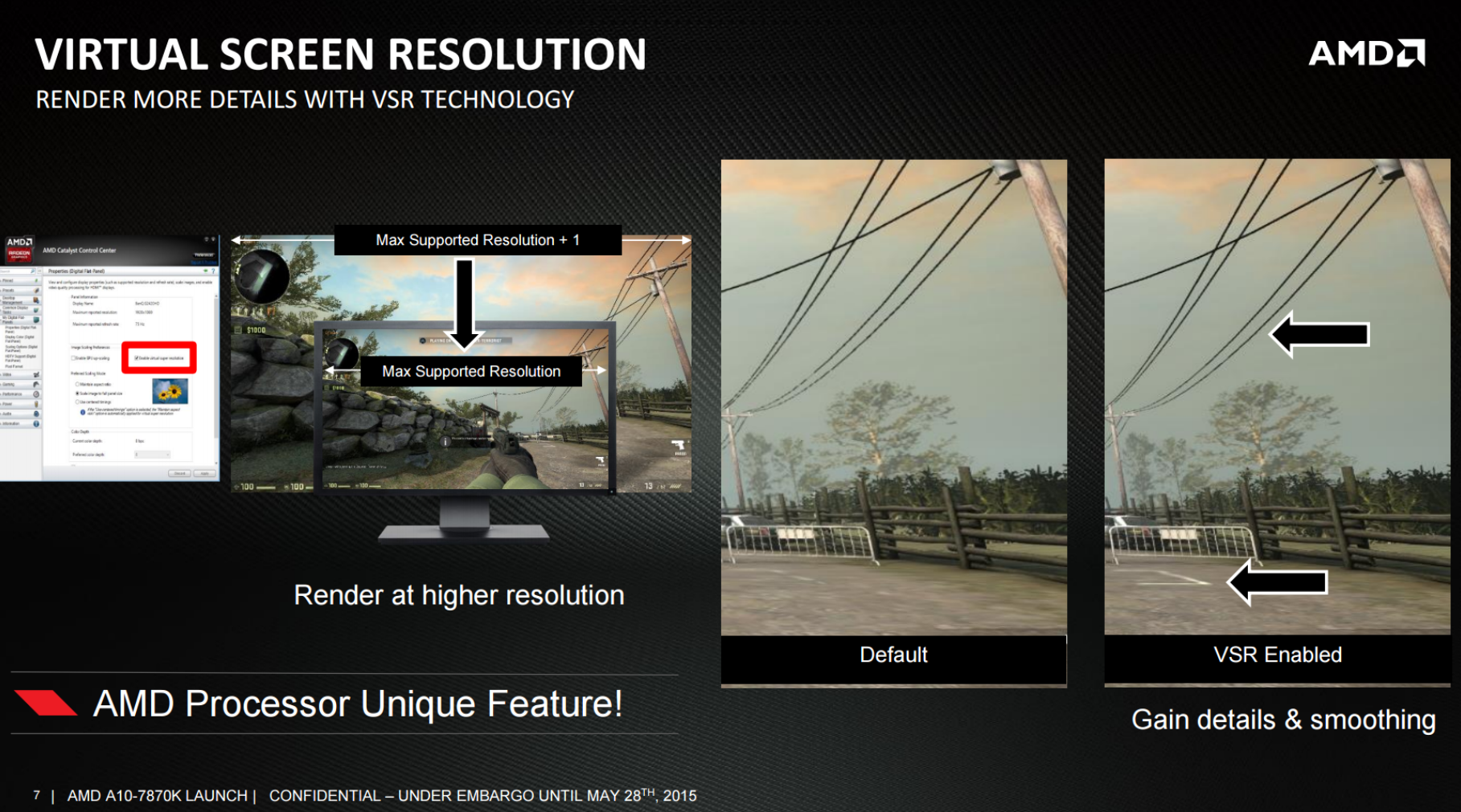
Similar to DSR, Virtual Screen Resolution is a driver level feature that allows the APU to render at a resolution higher than the monitor is capable and then scale the resulting image down to the actual screen resolution. Benefits include better aliasing, allowing both in-rendering algorithms and post-processing to essentially work on a larger image, as shown above. Obviously this comes at a price, namely performance. On the APU side it might be argued that VSR is not a great technology as typically people will game at lower resolutions anyway, or at 1080p with low/medium details while being limited around the 30 FPS barrier. The main plus point would be for devices that are resolution limited, say 720p, allowing them to render 1080p offscreen and then scale back in.
Back to the A10-7870K specifically, AMD is stating that due to the Kaveri Refresh nature of the SKU, it will be suited to all FM2+ capable sockets and motherboards that conform to AMD’s specifications.
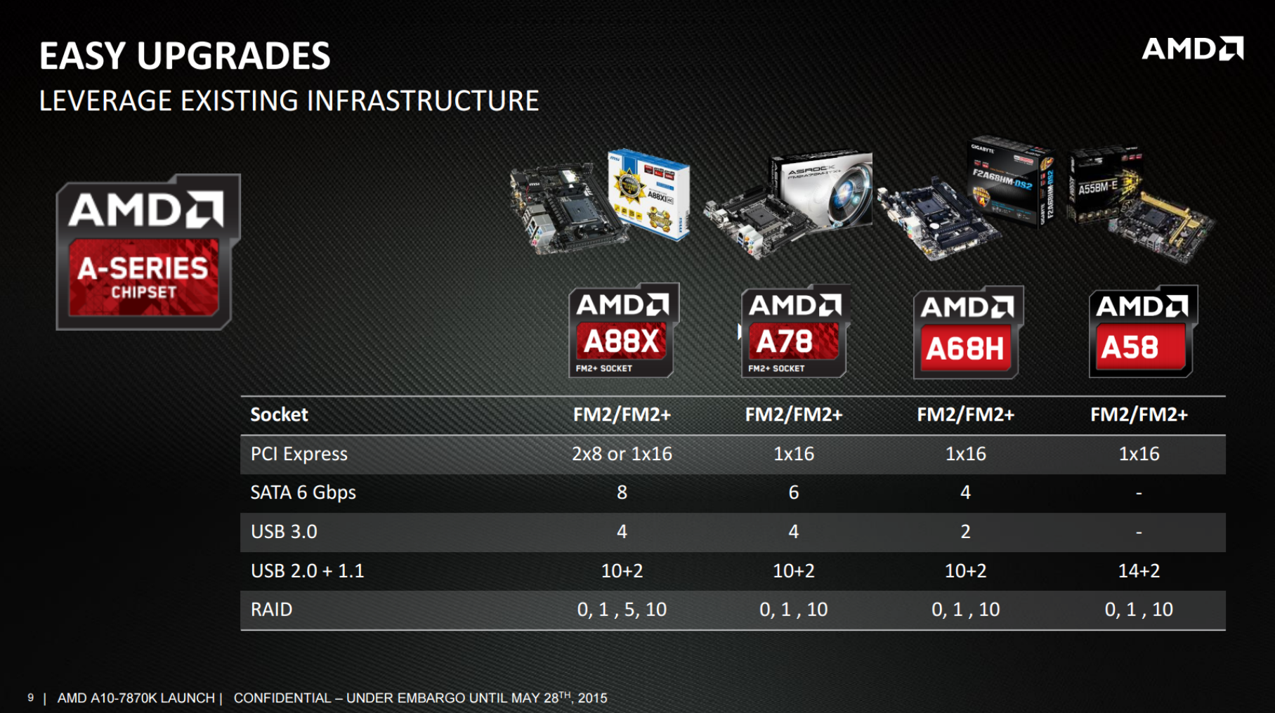
That last bit is particularly important, based on information I received from one of the motherboard manufacturers that specifically released new motherboards for Kaveri Refresh. The motherboard manufacturer stated that they released new motherboards because the power draw for the graphics portion of the APU is now more substantial than before, and they wanted to implement an element of security into their products. Needless to say, it allows OEMs and system builders to provide a ‘more up-to-date’ motherboard when providing systems around the A10-7870K, but AMD were quick to respond by saying words to the effect of ‘any motherboard on the A88X/A78/A68H/A58 chipsets that use an FM2/FM2+ to our specifications will work with the Kaveri Refresh line’. So there you go.
Other Kaveri Refresh Models and OEM Availability
As I mentioned at the top of the page, there are a number of supposed ‘leaks’ floating around the internet recently, with a larger-than-normal proportion of them being obvious fakes in recent months (perhaps there’s a sale on faked slides or something) and others being convincingly near the real thing without being confirmed by AMD. As a result, without direct confirmation from AMD, it’s hard to say what is real or not. Some websites will be stating that one or two or more APUs were released at the same time as the A10-7870K, but we’re only going to report here what we have been told directly by AMD in this instance.
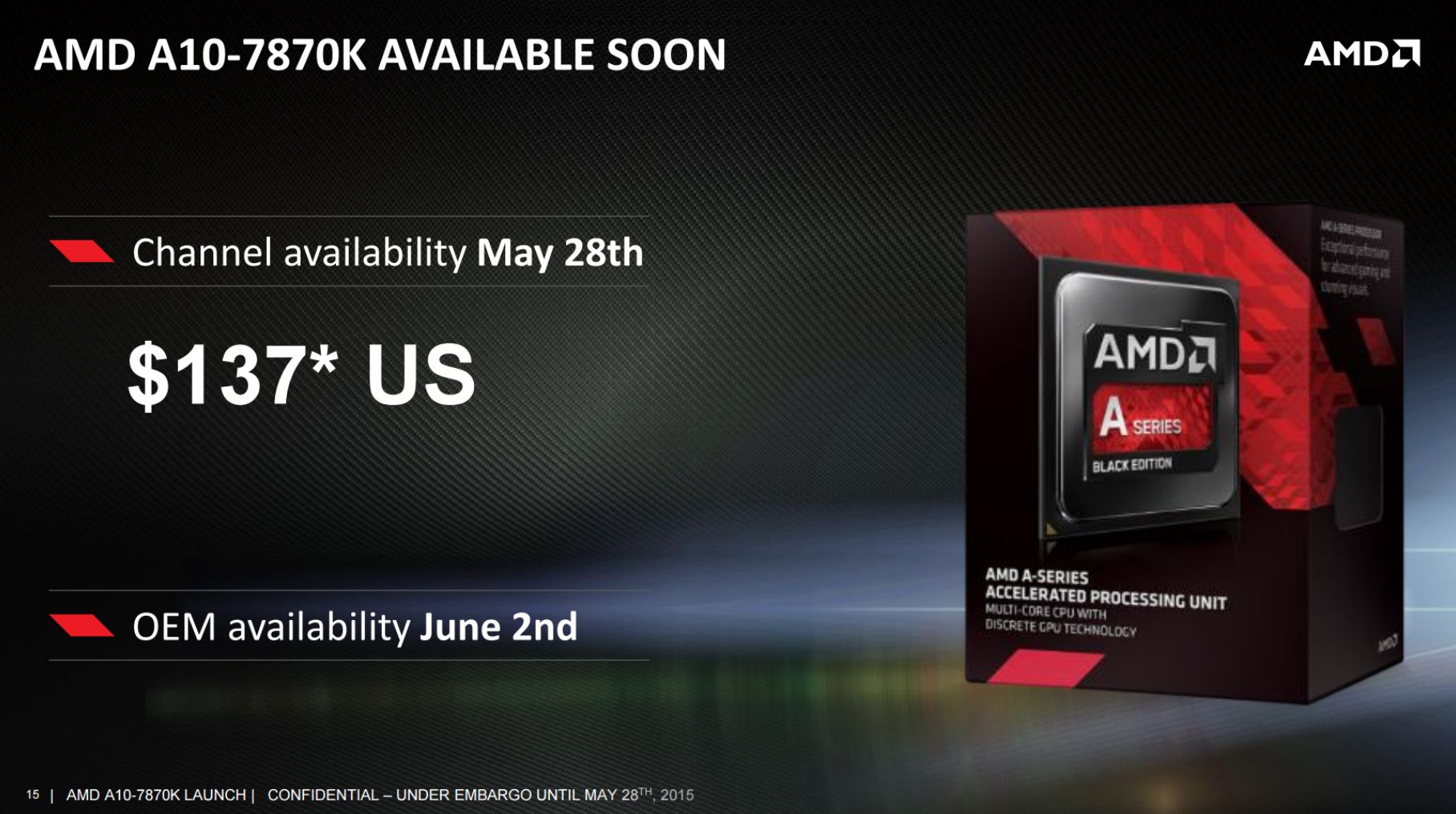
At present, only the A10-7870K was officially launched on May 28th, and will retail in the channel for $137. OEM availability for the A10-7870K will be on June 2nd. Over the next few quarters, several more members will be added to the Kaveri Refresh family for both consumer and commercial, with a different naming scheme coming to the commercial side to account for generational updates to AMD’s customers. The details of those models have not been officially released to the public, and personally I have only heard broad speculation or seen unconfirmed slide mockups.
This Review
As with our other APU coverage in recent weeks, we are taking the A10-7870K for a spin in both regular, office, professional and gaming tests as well as some basic overclocking. Unfortunately due to the timing we failed to finish the last one or two tests before travelling to Computex, but these results will be added to our database later in the month when we return. There’s still over 100+ new data points for the A10-7870K to cover, and as usual the more modern tests results will be compared to here in the review but all the data points, including legacy and long-term benchmarks such as Cinebench 10 and POV-Ray, are in our benchmark database Bench. Head over there for specific benchmark comparisons or select two processors for a direct A vs B shootout for common benchmark data.
Test Setup
| Test Setup | |
| Processor | AMD A10-7870K 2 Modules, 4 Threads 3.9 GHz Base, 4.1 GHz Turbo 95W, Initial List Price $137 |
| Motherboard | MSI A88X-G45 Gaming |
| DRAM | G.Skill RipjawsZ 4x4GB DDR3-2133 9-11-10 |
| Low End GPU | Integrated ASUS R7 240 2GB DDR3 Dual Graphics with R7 240 |
| Mid Range GPU | MSI R9 285 Gaming 2GB MSI GTX 770 Lightning 2GB |
| High End GPU | MSI R9 290X Gaming LE 4GB ASUS GTX 980 Strix 4GB |
| Power Supply | OCZ 1250W Gold |
| Storage Drive | Crucial MX200 1TB |
| Operating System | Windows 7.1 64-bit, Build 7601 |
| CPU Cooler | Cooler Master Nepton 140XL CLC |
Many thanks to...
We must thank the following companies for kindly providing hardware for our test bed:
Thank you to AMD for providing us with the R9 290X 4GB GPUs.
Thank you to ASUS for providing us with GTX 980 Strix GPUs and the R7 240 DDR3 GPU.
Thank you to ASRock and ASUS for providing us with some IO testing kit.
Thank you to Cooler Master for providing us with Nepton 140XL CLCs.
Thank you to Corsair for providing us with an AX1200i PSU.
Thank you to Crucial for providing us with MX200 SSDs.
Thank you to G.Skill and Corsair for providing us with memory.
Thank you to MSI for providing us with the GTX 770 Lightning GPUs.
Thank you to OCZ for providing us with PSUs.
Thank you to Rosewill for providing us with PSUs and RK-9100 keyboards.
Those that have read my last couple of reviews would have noticed that we recently incorporated a pair of AMD R9 290X graphics cards into our CPU testing. These were kindly provided by the AMD UK/EU office in order to give us a comparison point for high-end AMD discrete performance. They supplied two of the MSI R9 290X 4GB Gaming LE models, which is one of the more cost effective R9 290X models allowing a full 2816 SPs per card. We are using these cards in our game testing and both of them in Crossfire when it comes to Shadows of Mordor in 4K.
Load Delta Power Consumption
Power consumption was tested on the system while in a single NVIDIA GTX 770 configuration with a wall meter connected to the OCZ 1250W power supply. This power supply is Gold rated, and as I am in the UK on a 230-240 V supply, leads to ~75% efficiency > 50W, and 90%+ efficiency at 250W, suitable for both idle and multi-GPU loading. This method of power reading allows us to compare the power management of the UEFI and the board to supply components with power under load, and includes typical PSU losses due to efficiency.
We are reporting the power consumption difference when idle and during an initial OCCT load. This is slightly skewed by the adjustment up the efficiency chain of our power supply, showing lower power CPUs consuming a little more, but despite this the qualitative comparison is a still a good place to start.
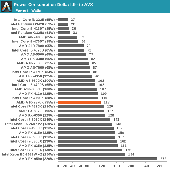
At 117W in our test, it seems a little over the 95W TDP listed, especially when the 7850K achieved 85W and under its 95W TDP. There will be variation within a SKU based on the binning quality, as I doubt the average 0.050 volts added to this SKU as I was told by AMD accounts for this much. Perhaps we ended up with a good 7850K sample but a mediocre 7870K sample. Alas with 100 CPUs we might get a better histogram of performance here, but we rarely get more than a single unit.


140 Comments
View All Comments
msroadkill612 - Thursday, May 23, 2019 - link
Your words are sage indeed sir. Reading them in 2019 it is clear how right you are. Of course your suggested combo is better buying for gaming performance.Cryio - Monday, June 1, 2015 - link
8320E? That's almost as expensive as the 8350.The best bang for the buck in AMD's portofolio is the 8300. Yes, you've read that right, 8300. Same TPD as the 8320E with some frequencies, same overclock capabilities and for 20% cheaper. It's only slightly more than an FX 6300.
Oxford Guy - Tuesday, June 2, 2015 - link
The 8320E is $100 from Microcenter.Cryio - Tuesday, June 2, 2015 - link
Then awesome. But generally, the 8300 is the cheapest you can buy.Dresdenboy - Monday, June 1, 2015 - link
What is the BIOS version being used? And what was the voltage?According to CPU World there might be heavy throttling with a somewhat older BIOS. The newer version fixes the problems:
"Update (May 31): Throttling problem was fixed by upgrading to P2.60 BIOS. Thanks to Roger Harshman for the hint! The processor is stable now, and runs CPU benchmarks and games without throttling and lockups. By the way, new BIOS sets lower core voltage, close to 1.45V."
Cryio - Monday, June 1, 2015 - link
The only thing that saddens me is that on average, the iGPU in the 7870K is still just 3 fps faster on average than a 240 DDR3.On paper, the iGPU should be as fast as a 7750 GDDR5 ! Not to mention the iGPU is based on GCN 1.1.
But for whatever reason, it's still 50% slower than it should be.
frozentundra123456 - Monday, June 1, 2015 - link
No, it has the same number of shaders as the 7750, but lower clocks, less bandwidth, and a limited thermal envelope. I don't know why you think it should be as fast as the 7750.Cryio - Monday, June 1, 2015 - link
Same number of shaders (both have 512), indeed lower clocks but newer architecture which should compensate for deficiencies.Plus 2400 DDR3 dual channel should allow it all the bandwidth in the world.
nikaldro - Tuesday, June 2, 2015 - link
Nope. GDDR5 is immensely better than any DDR3 on the planet, plus the APU has to throttle back due to the TDP constraints. NO WAY it will reach a 7750. the newer architecture isn't much faster, the main improvement are the added features.fallaha56 - Monday, June 1, 2015 - link
where is a DX12 preview? this is what is really needed to see which chip is the one to get...