The NVIDIA GeForce GTX 980 Ti Review
by Ryan Smith on May 31, 2015 6:00 PM ESTMeet The GeForce GTX 980 Ti
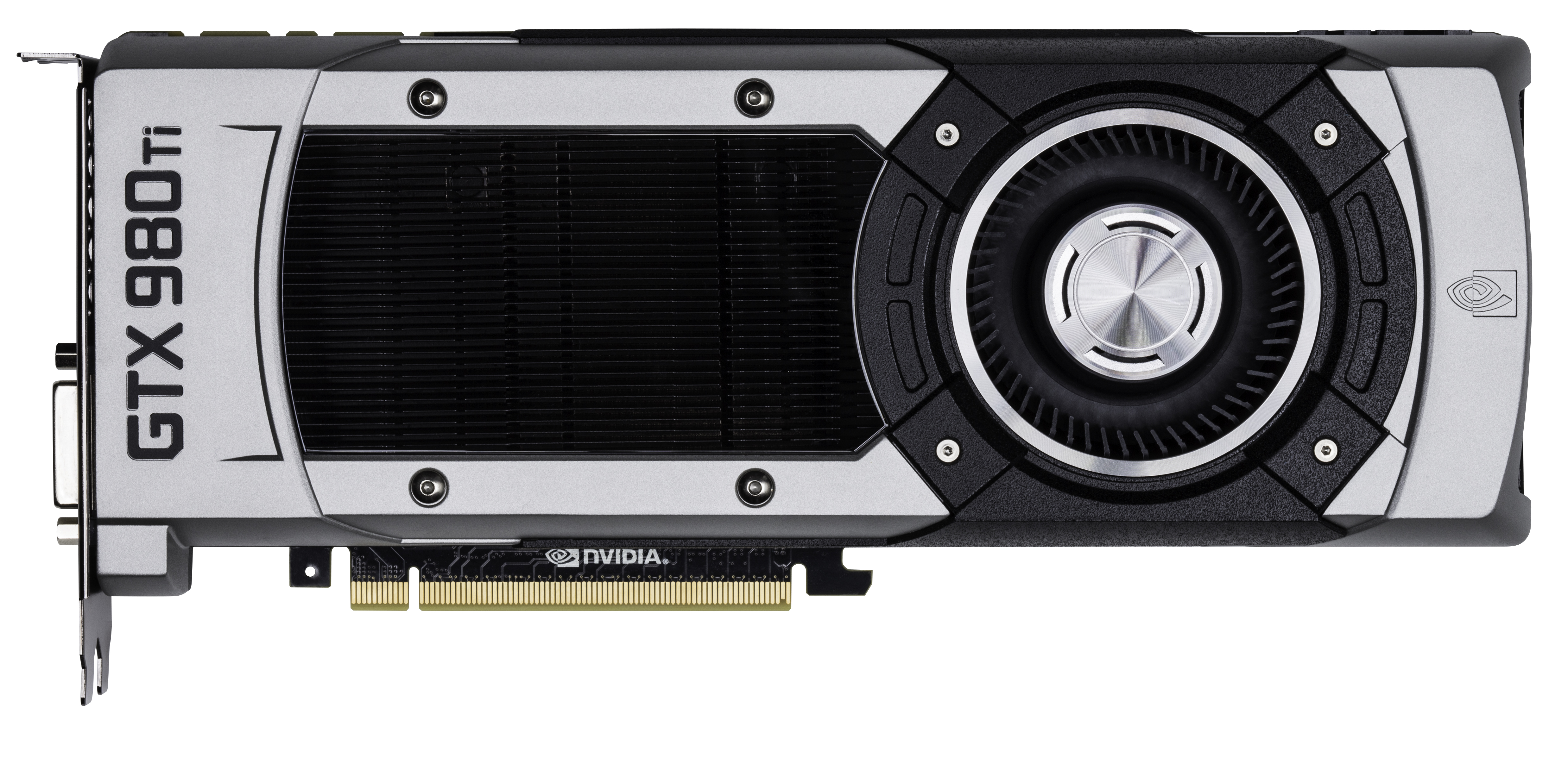
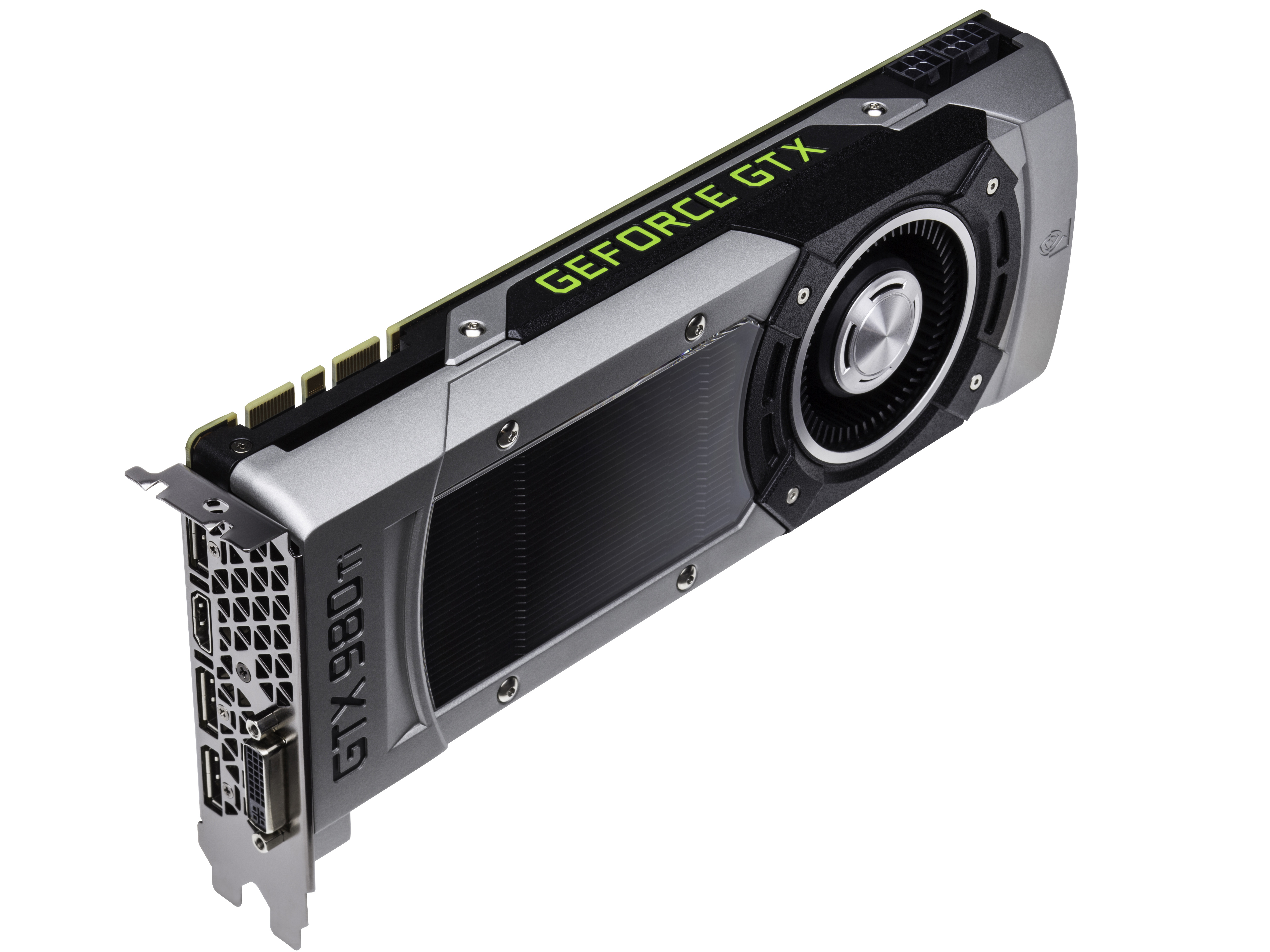
Like the rest of NVIDIA’s high-end cards in this generation, the reference GeForce GTX 980 Ti is launching with NVIDIA’s standard metal cooler. This design has served NVIDIA well since the launch of the GTX Titan in 2013 and continues to be the blower design to beat the high end, easily handling the 250W TDP of NVIDIA’s high-end cards without generating a ton of noise in the process.
As with so many other aspects of the GTX 980 Ti, the GTX 980 Ti’s cooler and build is a near-copy of the GTX Titan X. The only difference in the cooler is the paint job; GTX Titan X got a unique black paint job, while GTX 980 Ti gets the more standard bare aluminum finish with black lettering and a black-tinted polycarbonate window.
Otherwise there’s very little to be said about the GTX 980 Ti’s design that hasn’t been said before, so we’ll just recap what we said about the cooler design from our review of the GTX Titan X.
For GTX 980 Ti, NVIDIA has opted to leave well enough alone, having made virtually no changes to the shroud or cooling apparatus. And truth be told it’s hard to fault NVIDIA right now, as this design remains the gold (well, aluminum) standard for a blower. Looks aside, after years of blowers that rattled, or were too loud, or didn’t cool discrete components very well, NVIDIA is sitting on a very solid design that I’m not really sure how anyone would top (but I’d love to see them try).
In any case, our favorite metal shroud is back once again. Composed of a cast aluminum housing and held together using a combination of rivets and screws, it’s as physically solid a shroud as we’ve ever seen. The card measures 10.5” long overall, which at this point is NVIDIA’s standard size for high-end GTX cards.
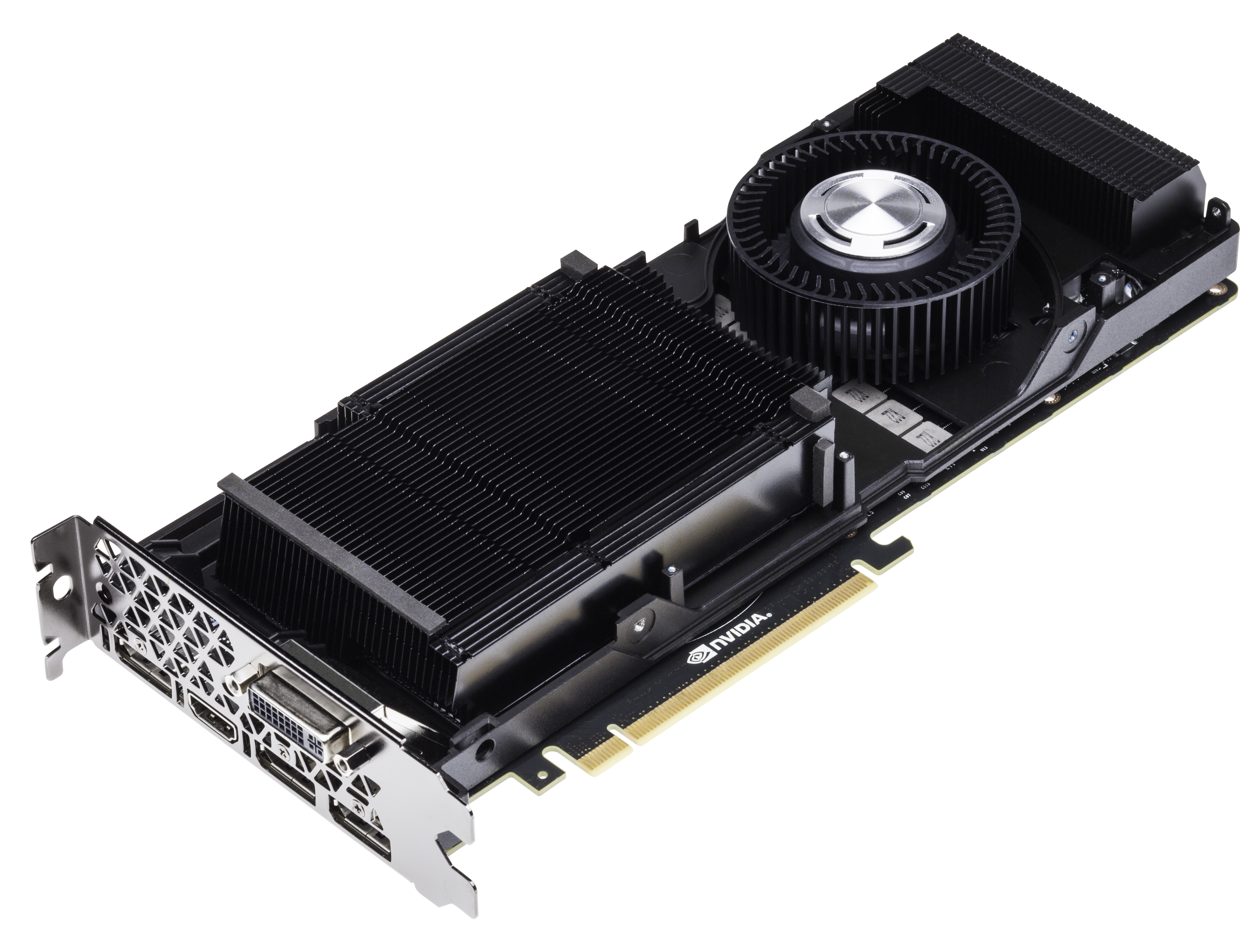
Drilling down we have the card’s primary cooling apparatus, composed of a nickel-tipped wedge-shaped heatsink and ringed radial fan. The heatsink itself is attached to the GPU via a copper vapor chamber, something that has been exclusive to NVIDIA’s 250W cards and provides the best possible heat transfer between the GPU and heatsink. Meanwhile the rest of the card is covered with a black aluminum baseplate, providing basic heatsink functionality for the VRMs and other components while also protecting them.
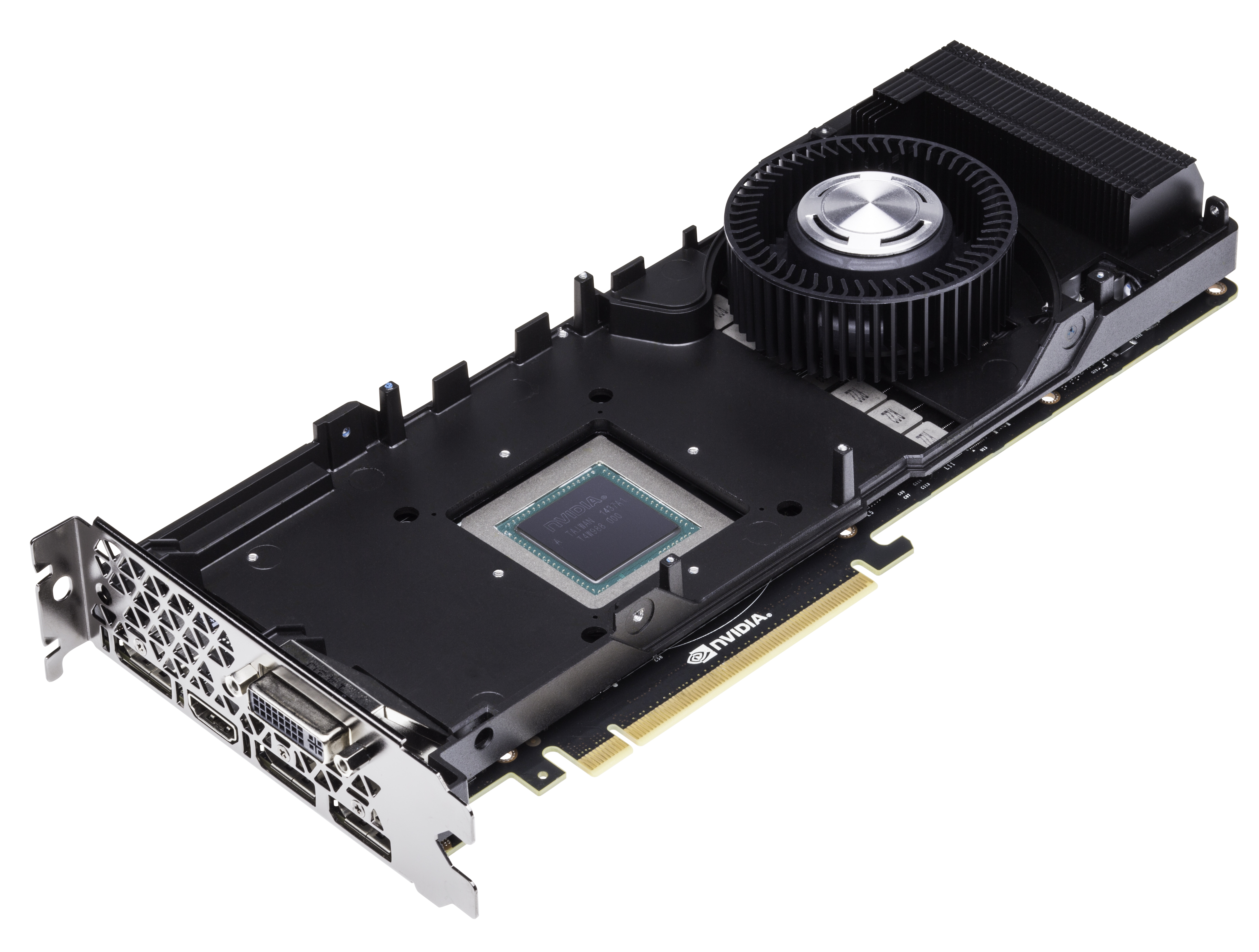
Finally at the bottom of the stack we have the card itself, complete with the GM200 GPU, VRAM chips, and various discrete components. The GM200 PCB places the GPU and VRAM chips towards the front of the card, while the VRMs and other discrete components occupy the back. As with the GTX Titan X, GTX 980 Ti features NVIDIA’s reworked component placement to improve airflow to the discrete components and reduce temperatures, along with employing molded inductors.
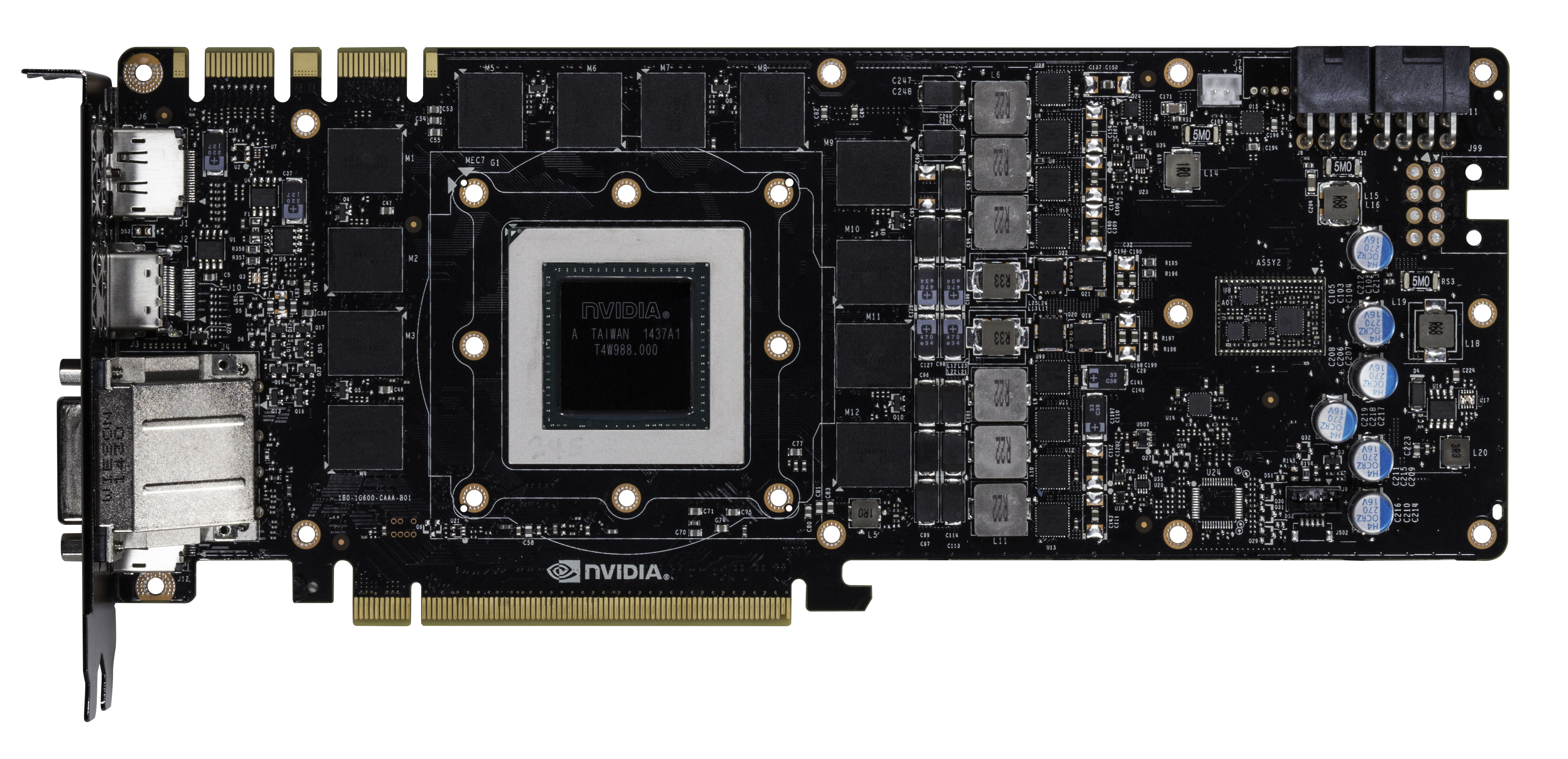
NVIDIA once again employs a 6+2 phase VRM design, with 6 phases for the GPU and another 2 for the VRAM. This means that GTX 980 Ti has a bit of power delivery headroom – NVIDIA allows the power limit to be increased by 10% to 275W – but hardcore overclockers will find that there isn’t an extreme amount of additional headroom to play with. Based on our sample the actual shipping voltage at the max boost clock is a bit higher than GTX Titan X, coming in at 1.187v, so in non-TDP constrained scenarios there is some additional headroom through overvolting, up to 1.23v in the case of our sample.
In terms of overall design, unlike GTX Titan X and its 24 VRAM chips, for the GTX 980 Ti NVIDIA only needs to use 12 VRAM chips to get the card’s 6GB of VRAM, so all of the VRAM is located at the front of the card. Halving the RAM capacity simplifies the card a bit – there are now no critical components on the back – and it brings down the total VRAM power consumption slightly. However despite this, NVIDIA has not brought back the backplate from the GTX 980, having removed it on the GTX Titan X due to the VRAM chips it placed on the rear.
Moving on, in accordance with GTX 980 Ti’s 250W TDP and the reuse of the metal cooler, power delivery for the GTX 980 Ti is identical to its predecessors. This means a 6-pin and an 8-pin power connector at the top of the card, to provide up to 225W, with the final 75W coming from the PCIe slot.
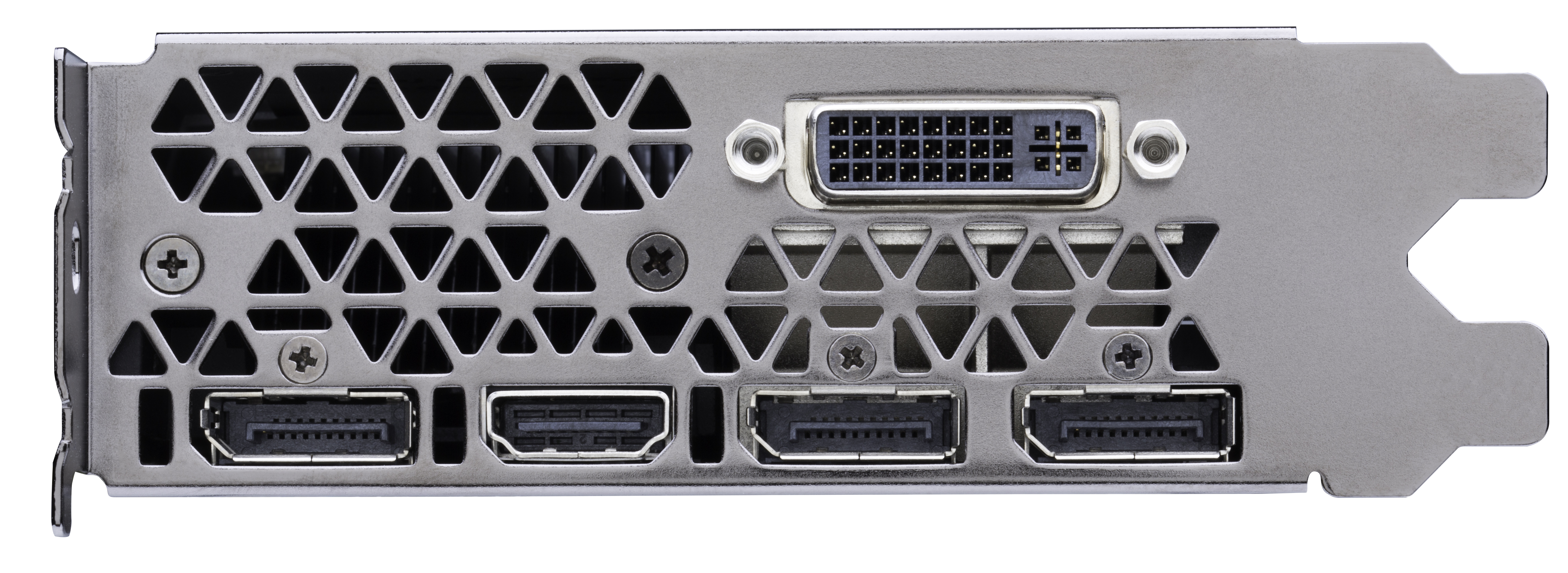
Meanwhile display I/O follows the same configuration we’ve seen on the rest of the high-end GTX 900 series. This is 1x DL-DVI-I, 3x DisplayPort 1.2, and 1x HDMI 2.0, with a total limit of 4 displays. In the case of GTX 980 Ti the DVI port is somewhat antiquated at this point – the card is generally overpowered for the relatively low maximum resolutions of DL-DVI – but on the other hand the HDMI 2.0 port is actually going to be of some value here since it means GTX 980 Ti can drive a 4K TV. Meanwhile if you have money to spare and need to drive more than a single 4K display, GTX 980 Ti also features a pair of SLI connectors for even more power.
Finally, taking a look at the long term, I wanted to quickly hit upon the subject of the VRAM capacity difference between the GTX 980 Ti and the GTX Titan X. Essentially NVIDIA’s only remaining selling point for the GTX Titan X, the Titan will remain their only 12GB card for some time to come. For NVIDIA this means that they can pitch the GTX Titan X as a more future-proof card than the GTX 980 Ti, as it would be hard-pressed to run out of VRAM.
The question for the moment then is whether 12GB is worth a higher premium, let alone the GTX Titan X’s $350 premium. The original GTX Titan by comparison was fortunate enough to come out with 6GB right before the current-generation consoles launched, and with them their 8GB memory configurations. This lead to a rather sudden jump in VRAM requirements in games that the GTX Titan was well positioned to handle, whereas GTX 780 Ti and its 3GB of VRAM can struggle in the very latest games at 4K resolutions. Much like 6GB in 2013, 12GB is overkill in 2015, all the while 6GB is a more practical amount for a 384-bit card at this time.
But to answer the question at hand, unlike the original GTX Titan, I suspect 12GB will remain overkill for a much longer period of time, especially without a significant technology bump like the consoles to drive up VRAM requirements. And consequently I don’t expect GTX 980 Ti to have any real issues with VRAM capacity in games over the next couple of years, making it better off than the GTX 780 Ti, relatively speaking.


290 Comments
View All Comments
przemo_li - Monday, June 1, 2015 - link
Fiji is NOT gpu name.Its gpu segment name.
Just like VI, SI, and some more.
Its chip name if anything.
If we for a moment switched to CPU-speak, You just claimed that Puma is single CPU from AMD ;)
Refuge - Monday, June 1, 2015 - link
It is the name of a GPU Architecture. Which could be a one run chip, or it could have multiple versions based on binning.dragonsqrrl - Monday, June 1, 2015 - link
It's not a GPU architecture. GCN is a GPU architecture, Maxwell is a GPU architecture. Fiji is a GPU, GM204 is a GPU. This isn't exactly a new paradigm we're dealing with here. Oh dear, I think I might be telling someone something (aka trolling***). I've done it again.dragonsqrrl - Wednesday, June 3, 2015 - link
First, that's a terrible analogy. Puma is not a CPU, it's a CPU architecture, successor to Jaguar. Fiji is a GPU, I never once assumed or suggested that there will be a single Fiji SKU (that was all you), right now it's likely there will be 2 for the consumer market.I'm honestly not sure what you meant by "segment", perhaps you could clarify? Are you talking about AMD's XT/PRO convention? They're still the same GPU, pro is typically just a harvested XT.
Refuge - Monday, June 1, 2015 - link
They released more than four if you include mobile GPU's I believe it goes up 2 more to 6.dragonsqrrl - Monday, June 1, 2015 - link
What do you mean mobile GPU's? Are you talking about the 900m series? There are no mobile specific GPU's in that lineup. It's all binned GM204 and GM107 SKU's.eanazag - Sunday, May 31, 2015 - link
Interesting observation. I see the same behavior, but the situations are different. Both major graphics vendors are stuck on 28 nm. The 285 is a new product. AMD's graphic situation is not even close to the same as CPU. They are not even competitive in most of the markets for CPU. AMD will likely release a very competitive GPU, which is why NV is releasing the Ti now.dragonsqrrl - Sunday, May 31, 2015 - link
Yes, the 285 is a new product, and while it is an improvement and a step in the right direction, Tonga just isn't enough to address the issue of AMD's profit margins this coming generation, or make them anymore competitive in mobile (M295X). It would be as though Nvidia were selling the 980 at the $200 price point. Not exactly, but from a memory interface, die size, PCB complexity, power consumption perspective, that's basically what AMD is doing right now, with no solution forthcoming. But I guess it's better than selling Tahiti for $200."AMD's graphic situation is not even close to the same as CPU. They are not even competitive in most of the markets for CPU. AMD will likely release a very competitive GPU, which is why NV is releasing the Ti now."
Some might argue they aren't competitive in the dGPU market with Nvidia market share approaching 80%... some might say that's like Intel levels of dominance...
And I didn't say it's the same as their CPU situation, I said it's becoming more similar. While AMD will likely be competitive in raw performance, as I've tried to explain in my past 2 comments, that's kind of besides the point.
chizow - Sunday, May 31, 2015 - link
Yes, both are stuck on 28nm, but only Nvidia came out with a comprehensive ASIC line-up knowing we'd be stuck here for another 2 years (going back to 2H 2014). It is obvious now that AMD's cost-cutting in staff and R&D is starting to manifest itself as they simply can't keep up while losing ground on 2 fronts (CPU and GPU).The culmination of this will be AMD going to market with a full series of rebrands of mostly old parts going back to 2011 with a single new ASIC at the top of their stack, while Nvidia has fully laid out its arsenal with GM107 (1 SKU), GM206 (1 SKU), GM204 (2 SKU), and now GM200 (2 SKU).
Kevin G - Monday, June 1, 2015 - link
Is it unprecedented? I recall the Geforce 9000, GTS 100 and most of the GTX 200 series being various rebrands from 'generation' to 'generation'. In fact, the 8800GTS 512 MB, 9800GTX, GTS 150 and GTS 250 were all the same chip design (the GTS 250 had a die shrink but was functionally unchanged).nVidia has gotten better since then, well with the exception of the GF108 that plagued the low end for far too long.