The NVIDIA GeForce GTX 980 Ti Review
by Ryan Smith on May 31, 2015 6:00 PM ESTPower, Temperature, & Noise
As always, last but not least is our look at power, temperature, and noise. Next to price and performance of course, these are some of the most important aspects of a GPU, due in large part to the impact of noise. All things considered, a loud card is undesirable unless there’s a sufficiently good reason – or sufficiently good performance – to ignore the noise.
As the GM200 flagship card, GTX Titan X gets the pick of the litter as far as GM200 GPUs go. GTX Titan X needed fully-functional GM200 GPUs, and even then needed GPUs that were good enough to meet NVIDIA’s power requirements. GTX 980 Ti on the other hand, as a cut-down/salvage card, gets second pick. So we expect to see these chips be just a bit worse; to have either functional units that came out of the fab damaged, or have functional units that have been turned off due to power reasons.
| GeForce GTX Titan X/980 Voltages | ||||
| GTX Titan X Boost Voltage | GTX 980 Ti Boost Voltage | GTX 980 Boost Voltage | ||
| 1.162v | 1.187v | 1.225v | ||
Looking at voltages, we can see just that in our samples. GTX 980 Ti has a slightly higher boost voltage – 1.187v – than our GTX Titan X. NVIDIA sometimes bins their second-tier cards for lower voltage, but this isn’t something we’re seeing here. Nor is there necessarily a need to bin in such a manner since the 250W TDP is unchanged from GTX Titan X.
| GeForce GTX 980 Ti Average Clockspeeds | |||
| Game | GTX 980 Ti | GTX Titan X | |
| Max Boost Clock | 1202MHz | 1215MHz | |
| Battlefield 4 |
1139MHz
|
1088MHz
|
|
| Crysis 3 |
1177MHz
|
1113MHz
|
|
| Mordor |
1151MHz
|
1126MHz
|
|
| Civilization: BE |
1101MHz
|
1088MHz
|
|
| Dragon Age |
1189MHz
|
1189MHz
|
|
| Talos Principle |
1177MHz
|
1126MHz
|
|
| Far Cry 4 |
1139MHz
|
1101MHz
|
|
| Total War: Attila |
1139MHz
|
1088MHz
|
|
| GRID Autosport |
1164MHz
|
1151MHz
|
|
| Grand Theft Auto V |
1189MHz
|
1189MHz
|
|
The far more interesting story here is GTX 980 Ti’s clockspeeds. As we have pointed out time and time again, GTX 980 Ti’s gaming performance trails GTX Titan X by just a few percent, this despite the fact that GTX 980 Ti is down by 2 SMMs and is clocked identically. On paper there is a 9% performance difference that in the real world we’re not seeing. So what’s going on?
The answer to that is that what GTX 980 Ti lacks in SMMs it’s making up in clockspeeds. The card’s average clockspeeds are frequently two or more bins ahead of GTX Titan X, topping out at a 64MHz advantage under Crysis 3. All of this comes despite the fact that GTX 980 Ti has a lower maximum boost clock than GTX Titan X, topping out one bin lower at 1202MHz to GTX Titan X’s 1215MHz.
Ultimately the higher clockspeeds are a result of the increased power and thermal headroom the GTX 980 Ti picks up from halving the number of VRAM chips along with disabling two SMMs. With those components no longer consuming power or generating heat, and yet the TDP staying at 250W, GTX 980 Ti can spend its power savings to boost just a bit higher. This in turn compresses the performance gap between the two cards (despite what the specs say), which coupled with the fact that performance doesn't scale lineraly with SMM count or clockspeed (you rarely lose the full theoretical performance amount when shedding frequency or functional units) leads to the GTX 980 Ti trailing the GTX Titan X by an average of just 3%.
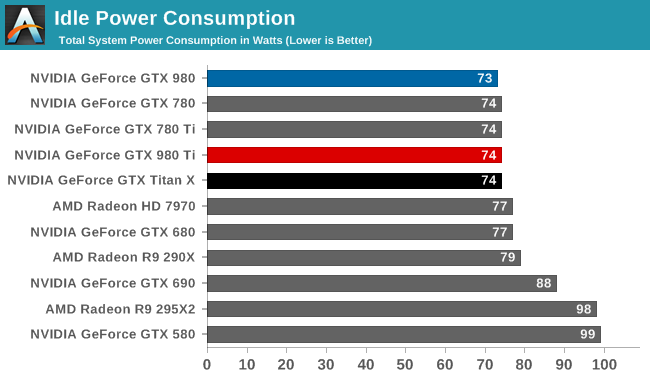
Starting off with idle power consumption, there's nothing new to report here. GTX 980 Ti performs just like the GTX Titan X, which at 74W is second only to the GTX 980 by a single watt.
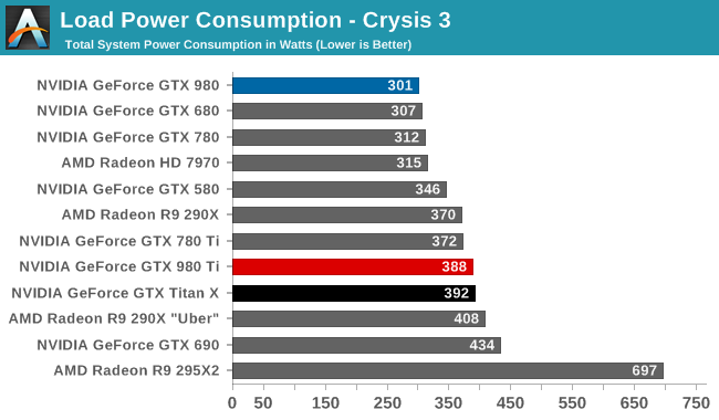
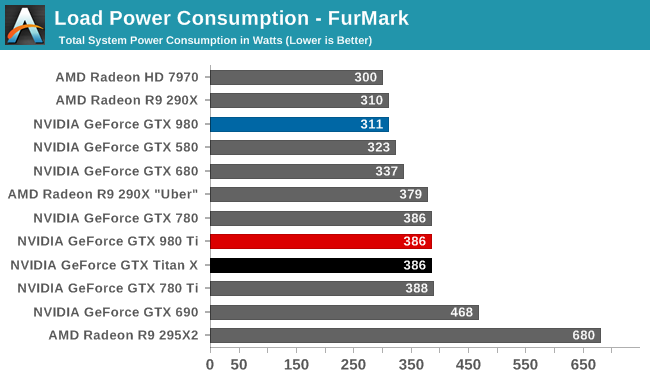
Meanwhile load power consumption is also practically identical to the GTX Titan X. With the same GPU on the same board operating at the same TDP, GTX 980 Ti ends up right where we expect it, next to GTX Titan X. GTX Titan X did very well as far as energy efficiency is concerned – setting a new bar for 250W cards – and GTX 980 Ti in turn does just as well.
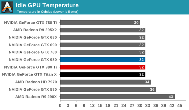
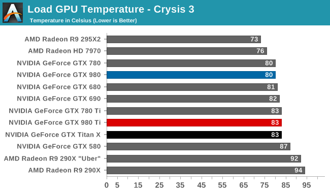
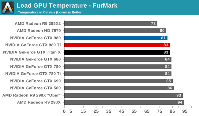
As was the case with power consumption, video card temperatures are similarly unchanged. NVIDIA’s metal cooler does a great job here, keeping temperatures low at idle while NVIDIA’s GPU Boost mechanism keeps temperatures from exceeding 83C under full load.
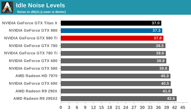
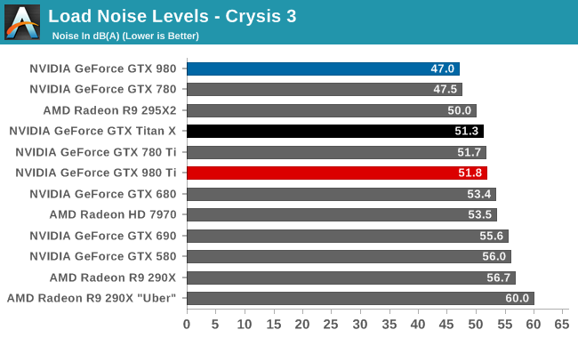
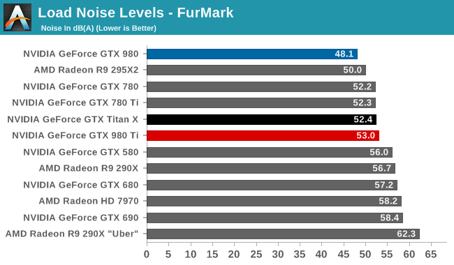
Finally for noise, the situation is much the same. Unexpected but not all that surprising, the GTX 980 Ti ends up doing a hair worse than the GTX Titan X here. NVIDIA has not changed the fan curves or TDP, so this ultimately comes down to manufacturing variability in NVIDIA’s metal cooler, with our GTX 980 Ti faring ever so slightly worse than the Titan. Which is to say that it's still right at the sweet spot for noise versus power consumption, dissipating 250W at no more than 53dB, and once again proving the mettle of NVIDIA's metal cooler.


290 Comments
View All Comments
przemo_li - Monday, June 1, 2015 - link
Fiji is NOT gpu name.Its gpu segment name.
Just like VI, SI, and some more.
Its chip name if anything.
If we for a moment switched to CPU-speak, You just claimed that Puma is single CPU from AMD ;)
Refuge - Monday, June 1, 2015 - link
It is the name of a GPU Architecture. Which could be a one run chip, or it could have multiple versions based on binning.dragonsqrrl - Monday, June 1, 2015 - link
It's not a GPU architecture. GCN is a GPU architecture, Maxwell is a GPU architecture. Fiji is a GPU, GM204 is a GPU. This isn't exactly a new paradigm we're dealing with here. Oh dear, I think I might be telling someone something (aka trolling***). I've done it again.dragonsqrrl - Wednesday, June 3, 2015 - link
First, that's a terrible analogy. Puma is not a CPU, it's a CPU architecture, successor to Jaguar. Fiji is a GPU, I never once assumed or suggested that there will be a single Fiji SKU (that was all you), right now it's likely there will be 2 for the consumer market.I'm honestly not sure what you meant by "segment", perhaps you could clarify? Are you talking about AMD's XT/PRO convention? They're still the same GPU, pro is typically just a harvested XT.
Refuge - Monday, June 1, 2015 - link
They released more than four if you include mobile GPU's I believe it goes up 2 more to 6.dragonsqrrl - Monday, June 1, 2015 - link
What do you mean mobile GPU's? Are you talking about the 900m series? There are no mobile specific GPU's in that lineup. It's all binned GM204 and GM107 SKU's.eanazag - Sunday, May 31, 2015 - link
Interesting observation. I see the same behavior, but the situations are different. Both major graphics vendors are stuck on 28 nm. The 285 is a new product. AMD's graphic situation is not even close to the same as CPU. They are not even competitive in most of the markets for CPU. AMD will likely release a very competitive GPU, which is why NV is releasing the Ti now.dragonsqrrl - Sunday, May 31, 2015 - link
Yes, the 285 is a new product, and while it is an improvement and a step in the right direction, Tonga just isn't enough to address the issue of AMD's profit margins this coming generation, or make them anymore competitive in mobile (M295X). It would be as though Nvidia were selling the 980 at the $200 price point. Not exactly, but from a memory interface, die size, PCB complexity, power consumption perspective, that's basically what AMD is doing right now, with no solution forthcoming. But I guess it's better than selling Tahiti for $200."AMD's graphic situation is not even close to the same as CPU. They are not even competitive in most of the markets for CPU. AMD will likely release a very competitive GPU, which is why NV is releasing the Ti now."
Some might argue they aren't competitive in the dGPU market with Nvidia market share approaching 80%... some might say that's like Intel levels of dominance...
And I didn't say it's the same as their CPU situation, I said it's becoming more similar. While AMD will likely be competitive in raw performance, as I've tried to explain in my past 2 comments, that's kind of besides the point.
chizow - Sunday, May 31, 2015 - link
Yes, both are stuck on 28nm, but only Nvidia came out with a comprehensive ASIC line-up knowing we'd be stuck here for another 2 years (going back to 2H 2014). It is obvious now that AMD's cost-cutting in staff and R&D is starting to manifest itself as they simply can't keep up while losing ground on 2 fronts (CPU and GPU).The culmination of this will be AMD going to market with a full series of rebrands of mostly old parts going back to 2011 with a single new ASIC at the top of their stack, while Nvidia has fully laid out its arsenal with GM107 (1 SKU), GM206 (1 SKU), GM204 (2 SKU), and now GM200 (2 SKU).
Kevin G - Monday, June 1, 2015 - link
Is it unprecedented? I recall the Geforce 9000, GTS 100 and most of the GTX 200 series being various rebrands from 'generation' to 'generation'. In fact, the 8800GTS 512 MB, 9800GTX, GTS 150 and GTS 250 were all the same chip design (the GTS 250 had a die shrink but was functionally unchanged).nVidia has gotten better since then, well with the exception of the GF108 that plagued the low end for far too long.