AMD Dives Deep On High Bandwidth Memory - What Will HBM Bring AMD?
by Ryan Smith on May 19, 2015 8:40 AM EST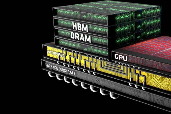
Though it didn’t garner much attention at the time, in 2011 AMD and memory manufacturer Hynix (now SK Hynix) publicly announced plans to work together on the development and deployment of a next generation memory standard: High Bandwidth Memory (HBM). Essentially pitched as the successor to GDDR, HBM would implement some very significant changes in the working of memory in order to further improve memory bandwidth and turn back the dial on memory power consumption.
AMD (and graphics predecessor ATI) for their part have in the last decade been on the cutting edge of adopting new memory technologies in the graphics space, being the first to deploy products based on the last 2 graphics DDR standards, GDDR4, and GDDR5. Consequently, AMD and Hynix’s announcement, though not a big deal at the time, was a logical extension of AMD’s past behavior in continuing to explore new memory technologies for future products. Assuming everything were to go well for the AMD and Hynix coalition – something that was likely, but not necessarily a given – in a few years the two companies would be able to bring the technology to market.
AMD Financial Analyst Day 2015
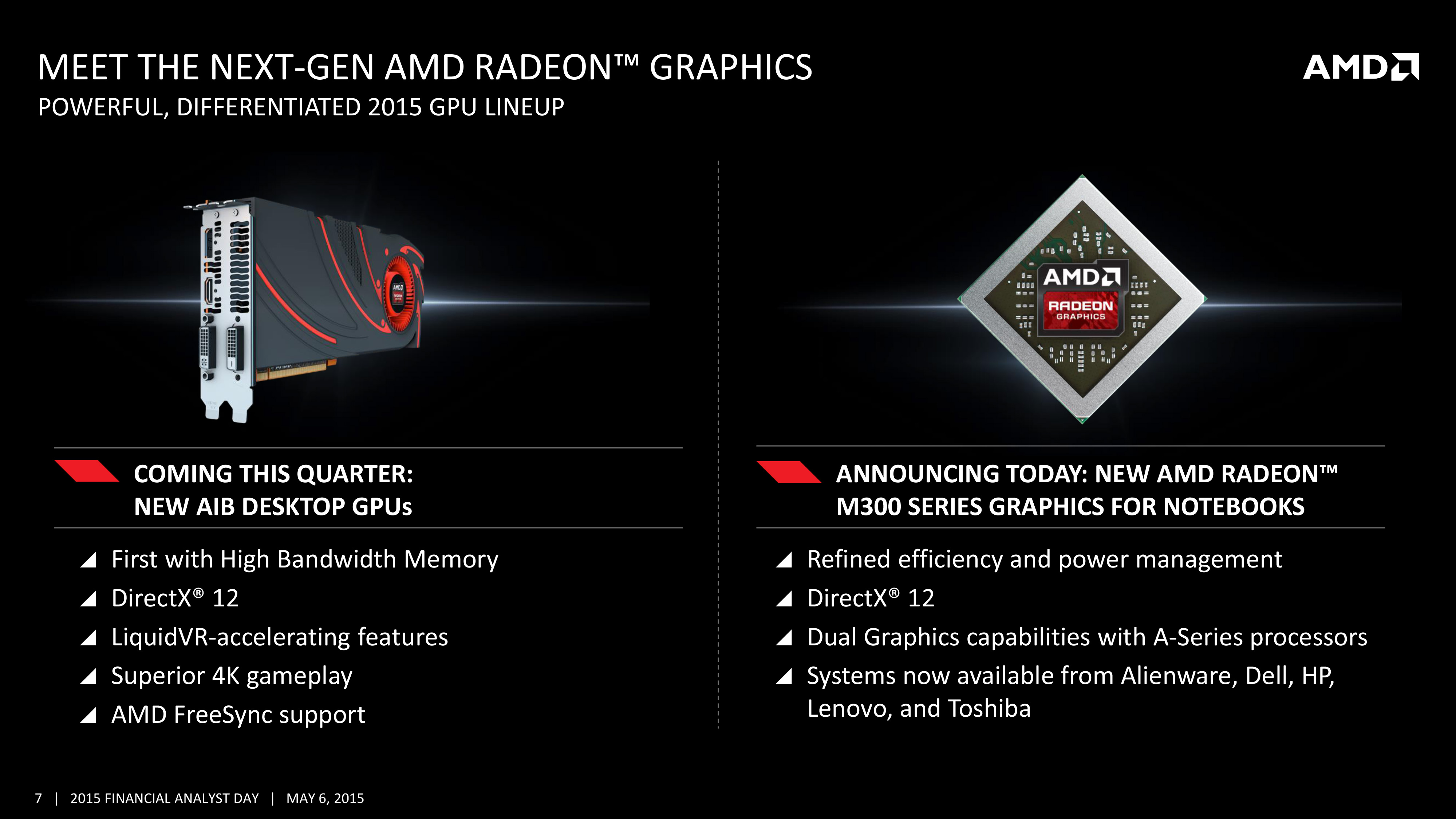
It’s now 4 years later, and successful experimentation has given way to productization. Earlier this month at AMD’s 2015 Financial Analyst day, the company announced that they would be releasing their first HBM-equipped GPU – the world’s first HBM-equipped GPU, in fact – to the retail market this quarter. Since then there have been a number of questions of just what AMD intends to do with HBM and just what it means for their products (is it as big of a deal as it seems?), and while AMD is not yet ready to reveal the details of their forthcoming HBM-equipped GPU, the company is looking to hit the ground running on HBM in order to explain what the technology is and what it can do for their products ahead of the GPU launch later that quarter.
To date there have been a number of presentations released on HBM, including by memory manufactures, the JEDEC groups responsible for shaping HBM, AMD, and even NVIDIA. So although the first HBM products have yet to hit retail shelves, the underpinnings of HBM are well understood, at least inside of engineering circles. In fact it’s the fact that HBM is really only well understood within those technical circles that’s driving AMD’s latest disclosure today. AMD sees HBM as a significant competitive advantage over the next year, and with existing HBM presentations having been geared towards engineers, academia, and investors, AMD is looking to take the next step and reach out to end-users about HBM technology.
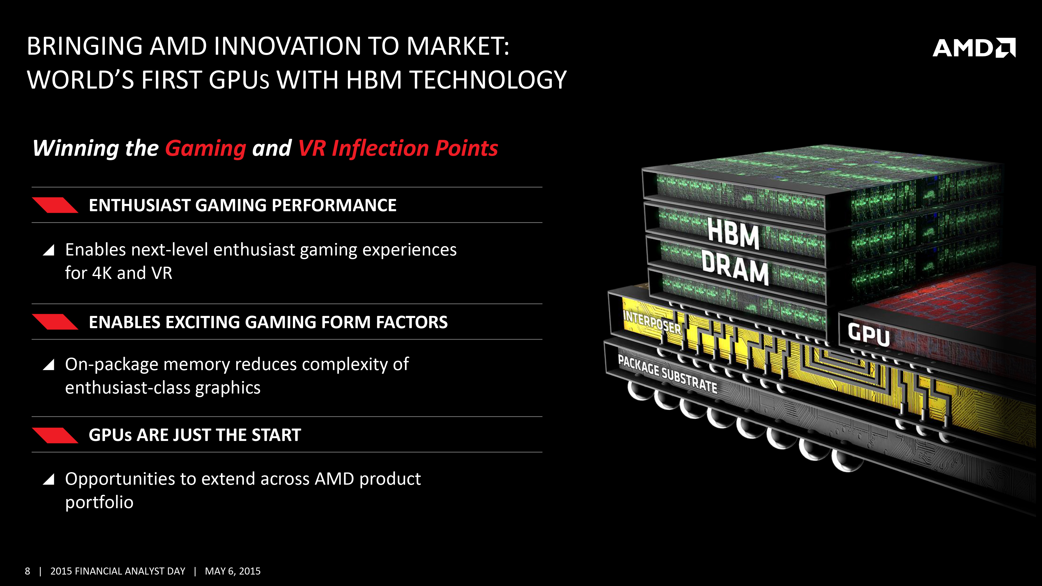
This brings us to the topic of today’s article: AMD’s deep dive disclosure on High Bandwidth Memory. Looking to set the stage ahead of their next GPU launch, AMD is reaching out to technical and gaming press to get the word out about HBM and what it means for AMD’s products. Ideally for AMD, an early disclosure on HBM can help to drum up interest in their forthcoming GPU before it launches later this quarter, but if nothing else it can help answer some burning questions about what to expect ahead of the launch. So with that in mind, let’s dive in.
I'd also like to throw out a quick thank you to AMD Product CTO and Corporate Fellow Joe Macri, who fielded far too many questions about HBM.


163 Comments
View All Comments
chizow - Wednesday, May 20, 2015 - link
lol @ trollranger101 doing what he does best, nothing.at80eighty - Thursday, May 21, 2015 - link
check any thread - he is predictable.chizow - Thursday, May 21, 2015 - link
Yes, predictably clearing up, refuting, and debunking the misinformation spread by...you guessed it. AMD fanboys like yourselves.Intel999 - Tuesday, May 19, 2015 - link
AMD has six months exclusivity on HBM1 since they co created it with Hynix. That is why no one else is using it yet.chizow - Wednesday, May 20, 2015 - link
Possibly, would make sense, and also explain why they are still going forward with it even if the 1st iteration isn't exactly optimal due to covered limitations (4GB, increased costs etc)SunLord - Tuesday, May 19, 2015 - link
HBM2 is supposed to double the bandwidth and density so 8GB of ram and 1TB/sec.... for a 4 chip setup it also seems to allow upto 32GB but HBM2 it isn't supposed to be ready till Q2 2016Kevin G - Tuesday, May 19, 2015 - link
Which is fine as the big 16/14 nm FinFET next generation chips aren't due to till around then anyway. The memory technology and foundry plans are aligning rather well.testbug00 - Tuesday, May 19, 2015 - link
Appears HBM2 increase it from 1GB to up to 4GB (2-4GB).Page 12:
http://www.hotchips.org/wp-content/uploads/hc_arch...
hans_ober - Tuesday, May 19, 2015 - link
How does temperature affect TSV's and the silicon interposer? Continuous thermal cycling usually stresses out joints. Wouldn't want one of the many thousand joints to break.Mr Perfect - Tuesday, May 19, 2015 - link
If I understand it correctly, joints usually suffer from thermal cycling because they are between different materials that heat and cool at different rates. The TSVs will be connecting silicon to silicon, so presumably the heating and cooling will be uniform and not stress the joints in that way.