MediaTek Unveils Helio X20 Tri-Cluster 10-Core SoC
by Andrei Frumusanu on May 12, 2015 4:00 AM EST- Posted in
- Smartphones
- Mobile
- MediaTek
- Cortex A72
- Helio
- Helio X20
- MT6597
Today MediaTek announces their brand new flagship SoC for smartphones and tablets, the Helio X20. MediaTek continues their Helio SoC branding announced earlier in the year, making the X20 the second SoC in the X-lineup and the first one to be actually released with the new product name from the beginning (as the X10 was a direct name change from the MT6795).
Right off the bat, MediaTek manages to raise eyebrows with what is the first 10 core System-on-a-Chip design. The 10 processor cores are arranged in a tri-cluster orientation, which is a new facet against a myriad of dual-cluster big.LITTLE heterogeneous CPU designs. The three clusters consist of a low power quad-core A53 cluster clocked at 1.4 GHz, a power/performance balanced quad-core A53 cluster at 2.0GHz, and an extreme performance dual-core A72 cluster clocked in at 2.5GHz. To achieve this tri-cluster design, MediaTek chose to employ a custom interconnect IP called the MediaTek Coherent System Interconnect (MCSI).
We'll get back to the new innovative CPU arrangement in a bit, but first let's see an overview of what the rest of SoC offers. MediaTek is proud to present its first CDMA2000 compatible integrated modem with the X20. This is an important stepping stone as the company attempts to enter the US market and try to breach Qualcomm's stronghold on the North American modems and SoCs. Besides C2K, the X20's modem allows for LTE Release 11 Category 6 with 20+20MHz Carrier Aggregation (downstream), supporting speeds up to 300Mbps in the downstream direction and 50Mbps upstream. The new modem also is supposed to use 30% less power when compared to the Helio X10.
The SoC also has an integrated 802.11ac Wi-Fi with what seems to be a single spatial stream rated in the spec sheets up to 280Mbps.
| MediaTek Helio X20 vs The Competition | ||||
| SoC | MediaTek Helio X20 (MT6797) |
MediaTek Helio X10 (MT6795) |
Qualcomm Snapdragon 808 (MSM8992) |
Qualcomm Snapdragon 620 (MSM8976) |
| CPU | 4x Cortex A53 @1.4GHz 4x Cortex A53 @2.0GHz 2x Cortex A72 @2.3-2.5GHz |
4x Cortex A53 @2.2GHz 4x Cortex A53 @2.2GHz |
4x Cortex A53 @1.44GHz 2x Cortex A57 @1.82GHz |
4x Cortex A53 @1.2GHz 4x Cortex A72 @1.8GHz |
| Memory Controller |
2x 32-bit @ 933MHz LPDDR3 14.9GB/s b/w |
2x 32-bit @ 933MHz LPDDR3 14.9GB/s b/w |
2x 32-bit @ 933MHz LPDDR3 14.9GB/s b/w |
2x 32-bit @ 933MHz LPDDR3 14.9GB/s b/w |
| GPU | Mali T8??MP4 @700MHz |
PowerVR G6200 @700MHz |
Adreno 418 @600MHz |
"Next-gen" Adreno |
| Encode/ Decode |
2160p30 10-bit H.264/HEVC/VP9 decode 2160p30 HEVC w/HDR encode |
2160p30 10-bit H.264/HEVC/VP9 decode 2160p30 HEVC encode |
2160p30, 1080p120 H.264 & HEVC decode 2160p30, 1080p120 H.264 encode |
2160p30, 1080p120 H.264 & HEVC
|
| Camera/ISP | Dual ISP 32MP @ 24fps |
13MP | Dual ISP 21MP |
Dual ISP 21MP |
| Integrated Modem |
LTE Cat. 6 300Mbps DL 50Mbps UL 2x20MHz C.A. (DL) |
LTE Cat. 4 150Mbps DL 50Mbps UL |
"X10 LTE" Cat. 9 450Mbps DL 50Mbps UL 3x20MHz C.A. (DL) |
"X8 LTE" Cat. 7 300Mbps DL 100Mbps UL 2x20MHz C.A. (DL & UL) |
Video encoding and decoding capabilities seem to be carried over from the MT6795 / X10, but MediaTek advertises a 30% and 40% improvement in decoding and encoding power consumption respectively.
Still on the multimedia side, we see the employment of a new integrated Cortex-M4 companion-core which serves as both an audio processor for low-power audio decoding, speech enhancement features and voice recognition, as well as sensor-hub function acting as a microcontroller for offloading sensor data processing from the main CPU cores. This means that while the device has the display turned off but is playing audio, only the M4 is in use in order to prolong battery life.
On the GPU side, the X20 seemed to be the first officially announced Mali T800 series GPU SoC. MediaTek explains that this is a still-unreleased ARM Mali high-end GPU similar to the T880. MediaTek initially chose a more conservative MP4 configuration clocked in at 700MHz, although final specifications are being withheld at this time. It should be noted that Mediatek has traditionally never aimed very high in terms of GPU configurations. It could be considered that the GPU in the X20 could still remain competitive in prolonged sustained loads as we saw larger Mali implementations such as Samsung's Exynos SoCs not being able to remain in the thermal envelope at their maximum rated frequencies. Initial relative estimates of the X20, expressed by MediaTek, compared to the Helio X10's G6200 see a 40% improvement in performance with a 40% drop in power.
On the memory side, MediaTek remains with a 2x32bit LPDDR3 memory interface running at 933MHz. MediaTek reasons that the SoC is limited to 1440p devices and the LPDDR3 memory should be plenty enough to satisfy the SoC's bandwidth requirements (a notion I agree with, given the GPU configuration).
Going back to the signature 10-Core/Tri-Cluster architecture of the SoC, MediaTek explains that this was a choice of power optimization over conventional two-cluster big.LITTLE designs. b.L works by employing heterogeneous CPU clusters - these may differ in architecture, but can also be identical architectures which then differ in their electrical characteristics and their target operating speeds. We've covered how power consumption curves behave in our Exynos 5433 deep-dive, and MediaTek presents a similar overview when explaining the X20's architecture.
One option in the traditional 2-cluster designs is to employ a low-power low-performance cluster, typically always a lower-power in-order CPU architecture such as ARM's A53. This is paired with a higher-power high-performance cluster, either a larger CPU core such as the A57/A72, or a frequency optimized A53 as we see employed in some past MediaTek SoCs, or most recently, HiSilicon's Kirin 930 found in the Huawei P8.
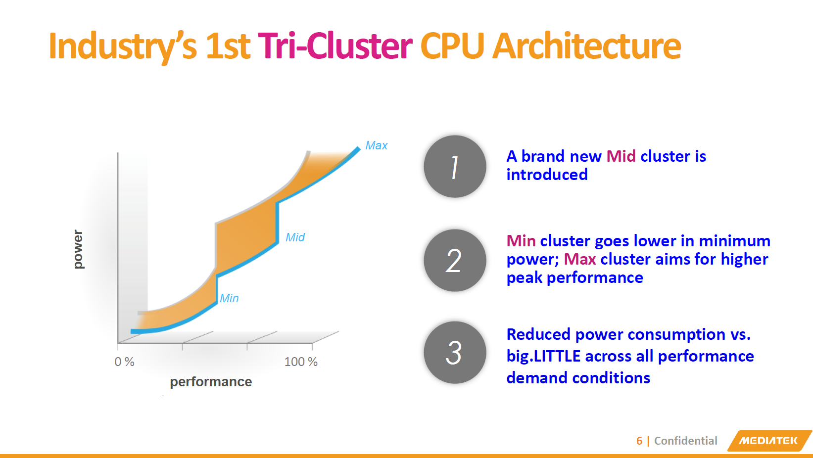
Contrary to what MediaTek presents as an "introduction of a Mid cluster", I like to see MediaTek's tri-cluster approach as an extension to the existing dual A53 cluster designs - where the added A72 cluster is truly optimized for only the highest frequencies. Indeed, we are told that the A72 cluster can reach up to 2.5GHz on a TSMC 20nm process. ARM aims similar clocks for the A72 but at only 14/16nm FinFET processes, so to see MediaTek go this high on 20nm is impressive, even if it's only a two-core cluster. It will be interesting to see how MediaTek chooses the lower frequency limits on each cluster, especially the A72 CPUs, or how these options will be presented to OEMs.
The end-result is a promised 30% improvement in power consumption over a similar 2-cluster approach. This happens thanks to the finer granularity in the performance/power curve and an increase in available performance-power points for the scheduler to place a thread on. Having a process that is heavy enough that it is not capable of residing on the smallest cluster due to performance constraints, but not demanding enough to require the big cluster's full performance, can now reside on this medium cluster at much greater efficiency than had it been running on the big cluster at reduced clocks. MediaTek uses CorePilot as a custom developed scheduler implementation that is both power aware and very advanced (based on our internal testing of other MediaTek SoCs). My experience and research with it on existing devices was fairly positive, so I'm sure the X20's new v3.0 implementation of CorePilot will be able to take good advantage of the tri-cluster design.
The biggest question and need of clarification is in the area of what the MCSI (the interconnect) is capable of. ARM had announced its CCI-500 interconnect back in February, which incidentally also promised the capability of up to 4 CPU clusters. MediaTek hinted that this may be a design based on ARM's CCI - but we're still not sure if this means a loosely based design or a direct improvement of ARM's IP. Cache coherence is a major design effort, and if MediaTek saw this custom IP as an effort worth committing to, then the MCSI may have some improvements we're still not clear on.

The Helio X20 is certainly an interesting SoC and I'm eager on how the tri-cluster design performs in practice. The X20 samples in H2 2015 and devices with it are planned to be shipping in Q1 2016. In the given time-frame, it seems the X20's primary competitor is Qualcomm's Snapdragon 620, so it'll be definitely a battle for the "super-mid" (as MediaTek likes to put it) crown.


69 Comments
View All Comments
mkaibear - Tuesday, May 12, 2015 - link
It's getting a bit like the gillete model now.Two clusters... no wait, 3 clusters!
...no wait! 4 clusters! Low, middle, high, eXtreme Performance!
...no wait! 5 clusters! With a lubricating strip!
Raniz - Tuesday, May 12, 2015 - link
Except that here it may actually make sense.close - Tuesday, May 12, 2015 - link
The main target isn't battery life, it's the marketing position. In a world where it's harder and harder to differentiate your product slapping on 2 more cores will put you on the radar. This is also true for resolution where you see ludicrously high resolutions on tiny panels (already talking about 4K).Plus it's a lot easier to slap on cores and some more RAM then it is to optimize your software and not have a "fart generator" type app that needs 50+MB of RAM or who knows how much CPU.
Apple must be doing something right with the iPhone 6 if they can fight a much beefier Galaxy S6 (with a huge difference in terms of cores, frequency and RAM) and still be competitive performance and battery wise. And I don't think it's "magic", it's just good hardware and software engineering.
menting - Tuesday, May 12, 2015 - link
Apple can optimize their CPU architecture to their needs only, and that's why they can compete well even with spec that is less on paper.Frenetic Pony - Tuesday, May 12, 2015 - link
Apple's needs for the Iphone are the exact same as anyone else's needs for a smartphone. They're just much better at CPU architecture than ARM. Which is why I'm more interested in seeing Qualcomm's newest Snapdragon later this year, as actual Core design seems far and away more important than any amount of clever SOC design, as Apple's 2 cores fits all and still beats 10 different cores strategy shows.dccafe - Wednesday, May 13, 2015 - link
Just so you know, Apple Iphones uses ARM architecture processors.The only difference are the add-on features, they are designed to better fit their software design.
rocketbuddha - Wednesday, May 13, 2015 - link
FP is correct.ARM is a ISA. The company also develops cores running its architecture under the Cortex moniker.
In general, QCOM, Marvel, Apple are companies that license the ISA, but design their own cores around it. NVIDIA tried the same with Denver, Not unlike AMD & INTC in the x86 world. Different designs running same/similar x64 ISA.
But other manufacturers license the ARM Cortex cores and its CPU system architecture, add other components to it and make a chip/SOC at different manufacturing nodes. Samsung, MediaTek, LG, Rockchip, NVIDIA, Huawei are in this category.
In the last generation QCOM hit the jackpot with the Krait core that was better at performance and power against the ARM Cortex A9 and better power/perf/die size advantage vs. ARM A15+A8 combination. With the modem related integration it basically whalloped competition.
Apple dropped their first bomb by designing their own Swift core with ARM v8 compatibility before even ARM was ready with its own Cortex implementation of v8 ISA.
QCOM pooh-poohed and missed the 64 bit bus very badly. But it had to rush the first generation 810, 610, 410, 808 in place by actually implementing Cortex A57 + Cortex A53 cores as Samsung and MDTK were expected to be ready before their custom QCOM's ARM v8 core was ready.
WinterCharm - Wednesday, May 13, 2015 - link
Except apple's ARM cores are custom designed, since they have the license to take liberties with the architecture.babadivad - Saturday, May 16, 2015 - link
Apple's cores are 100% custom. They don't take reference designs from ARMs Cortex CPU and modify them. They build them from scratch without any of ARM's input on design. But they did license the ARM ISA so their CPUs run ARM instructions [like Intel and AMD CPUs run x86].Jef.Holt - Thursday, August 13, 2015 - link
Apple has complete control of the entire system, unlike any other manufacture. Samsung comes closest with their SoC and building their own phones. But Apple has the CPU, phone and OS all under their control. This means Apple can create opcodes in silicon specifically to optimize iOS performance.So when you control the Integrated Development Environment (IDE), the hardware SOC (A9), the OS (iOS) and the additional components to make a turn key product, you can optimize every component to maximize the entire product performance. From the IDE perspective there is Metal and other tweaks under the hood that create tighter more efficient code. This code is so efficient that both Google and Microsoft have porting products out that take advantage of that same tight code to both improve performance of there phones and to quicken the porting process.
SoC the A7, A8 and A9. All of these chips have CPU, GPU and IPU, just to name a few, that can or do have Apple specific code to optimize the performance and efficiency that you must have total control to get. We can see this in the real world usage more than the Bench Marks because code is more often optimized for Apps than for the Bench Marks.
Other chips used. Apple can test multiple chips for efficiency in their specific designs to find the most efficient combinations, this maximizes the battery and allows for smaller lighter devices. Apple can also use features of the support chips much more efficiently because it can write the usage directly into the IDE. Other manufactures cannot do this because they use the monolithic Android OS that is written with the idea of all SoCs and all support chips.
All of these optimizations add up to added performance that we can see.