Inside OCZ's Factory: How SSDs Are Made
by Kristian Vättö on May 20, 2015 8:30 AM ESTThe Factory
OCZ's factory is located in Zhongli, which is a district of Taoyuan City, about a 45-minute drive away from the center of Taipei. Technically the factory is now owned and operated by Powertech Technology Inc (commonly known as PTI) because Toshiba wanted OCZ to sell the factory as a part of the acquisition. PTI is a relatively big name in the manufacturing industry with over 10,000 employees and a number of high value customers (including Apple, for instance). Aside from assembly, PTI also does wafer probing and die packaging and actually all Toshiba NAND is packaged by PTI (to my knowledge Samsung is the only NAND supplier that does all NAND packaging in-house), so the company has strong relationship with OCZ and Toshiba. While visiting the factory, I certainly got the feeling that OCZ and PTI are very well integrated as the cooperation between the two is effectively frictionless, which is partially explained by the fact that prior to the acquisition, the employees of the factory had paychecks directly from OCZ.
Two surface-mount technology (SMT) lines in the factory are dedicated to OCZ with a total capacity of approximately 70,000 units per month. OCZ also has burst capacity with other SMT lines and factories that PTI owns in case there's a sudden spike in demand (e.g. a large enterprise order). The facility has room for up to ten SMT lines and OCZ is looking to increase production capacity in the future. However, the factory isn't fully exclusive to OCZ as PTI does manufacture other vendors' drives too and during the tour I spotted some Kingston SSDs.
Assembling an SSD
Assembling an SSD isn't really any different from any other component that is built on a printed circuit board (PCB). The process itself is very straightforward and contains only a handful of steps which should be the same for every manufacturer.
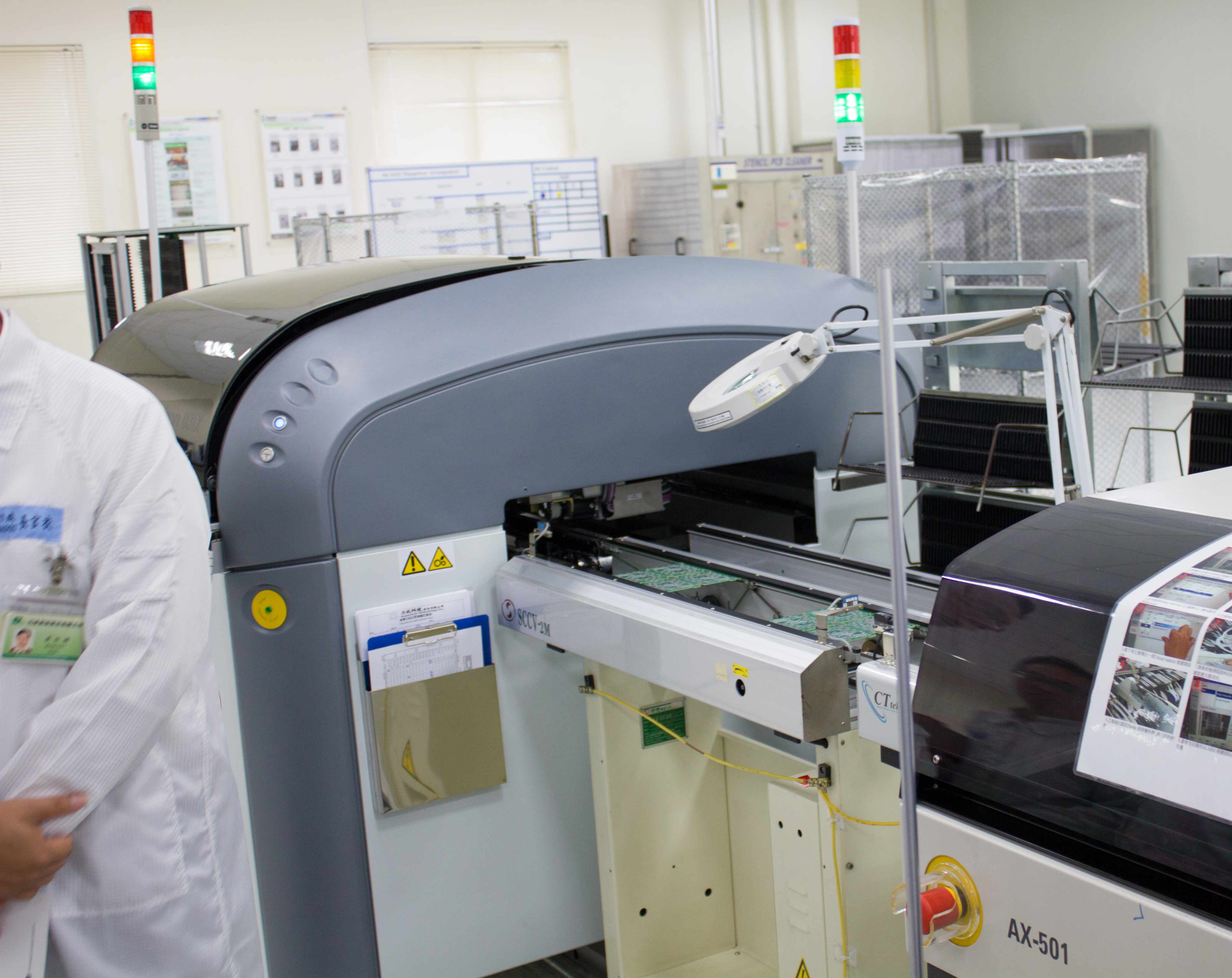
The process begins by printing the circuit board and coating the chip/resistor sockets with solder paste, which is done in the machine pictured above.
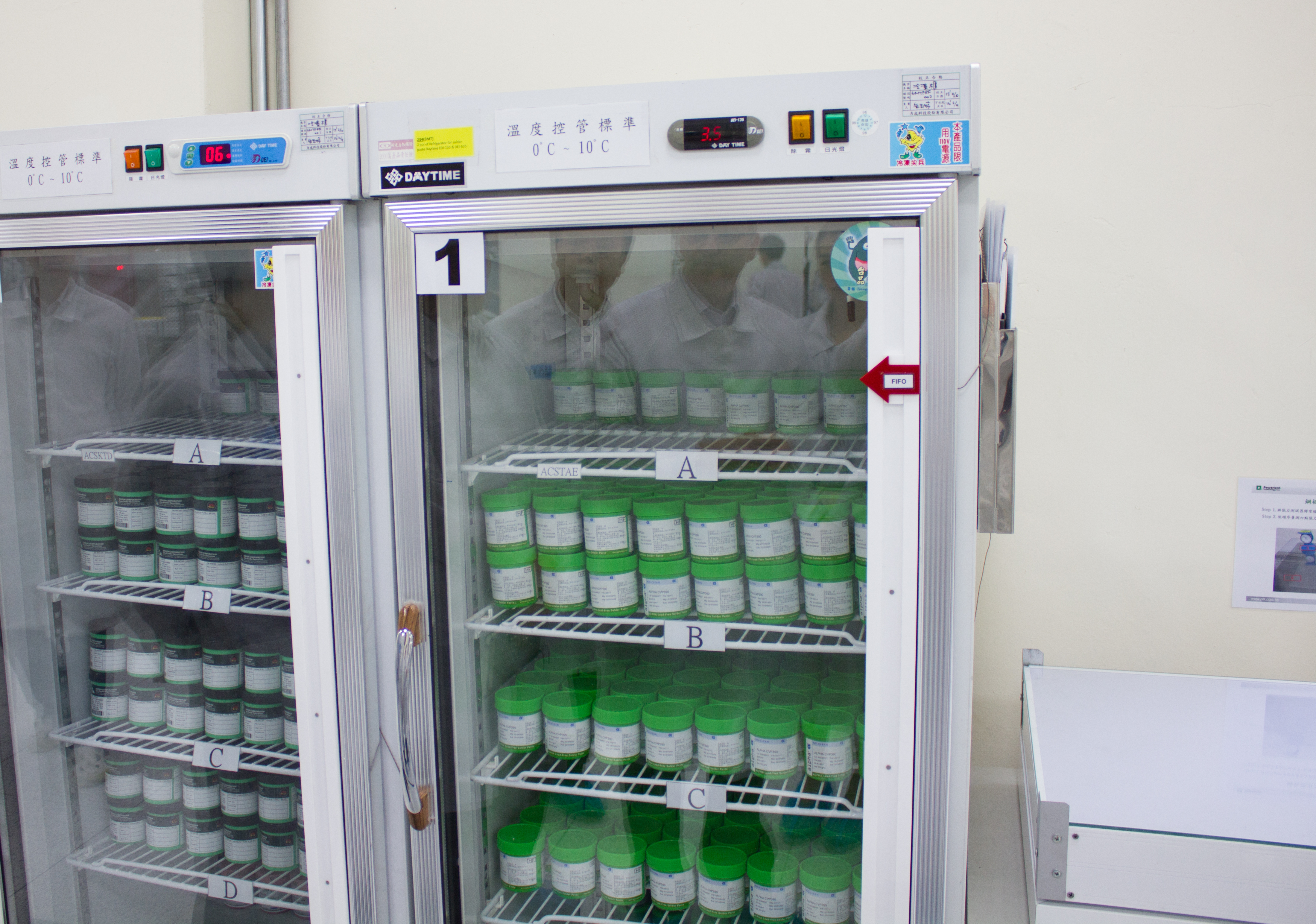
The solder paste must be stored in near-zero temperature at all times or otherwise it will lose its soldering characteristics. It can only withstand room temperature for a couple of hours before becoming waste, which is why the paste is stored in small cans to minimize the loss.

Once the PCB has been printed and solder paste applied, the end result is what's pictured above. Four 2.5" PCBs can be processed at the same time, but obviously a smaller PCB would result in higher throughput since more PCBs would fit in the same area and could be processed simultaneously for better cost efficiency. That's why we've seen some manufacturers adopting smaller PCBs in 2.5" drives.
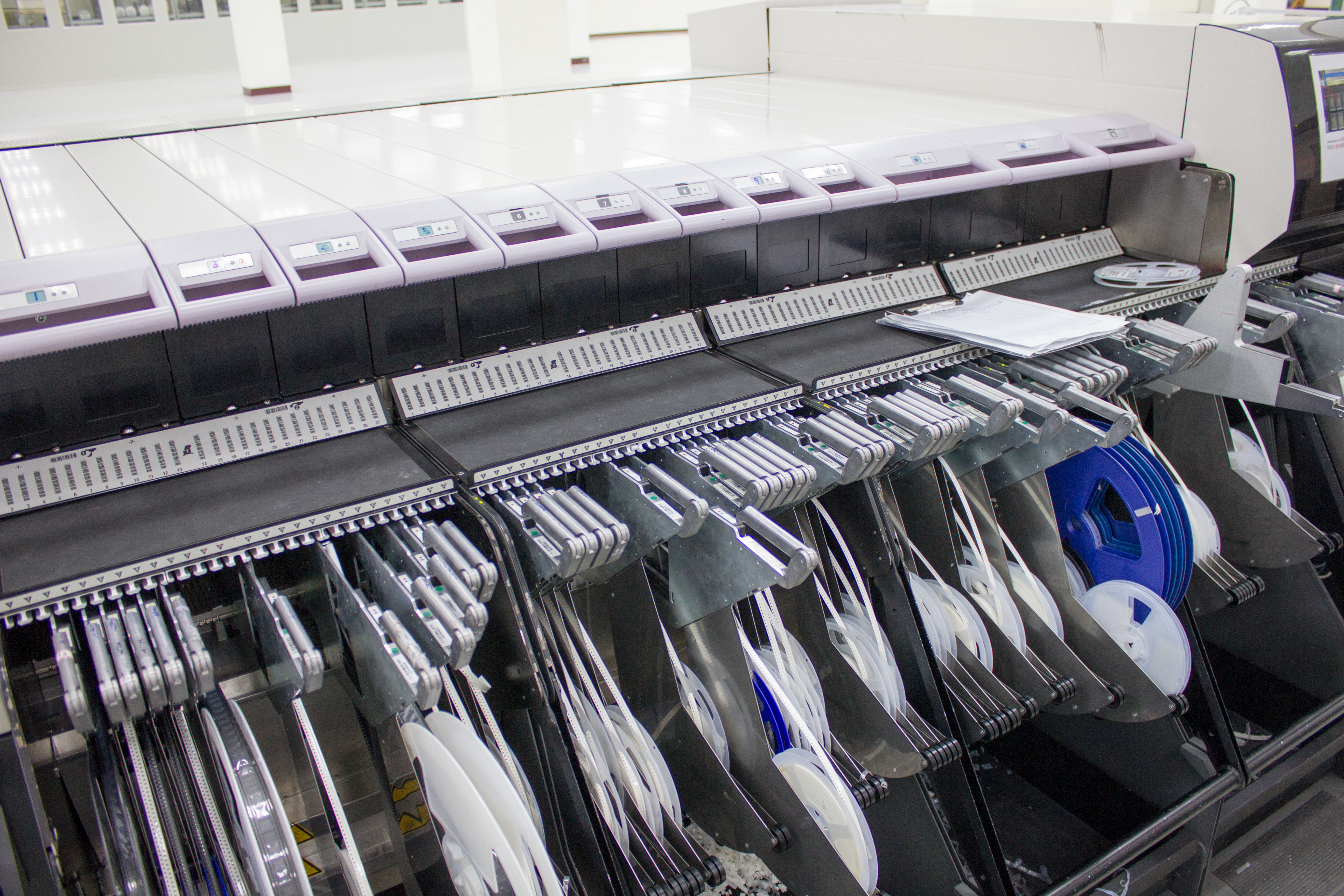
The PCB is now ready to take on the actual chips, which are mounted on the PCB by the above mounter. Every individual chip, resistor and capacitor is loaded to the machine in a circular "tape and reel" and the machine then automatically mounts the components to their right places on the PCB.

The controller come in a slightly different tray and it's the last component to be mounted before the drive moves to the cooking stage.
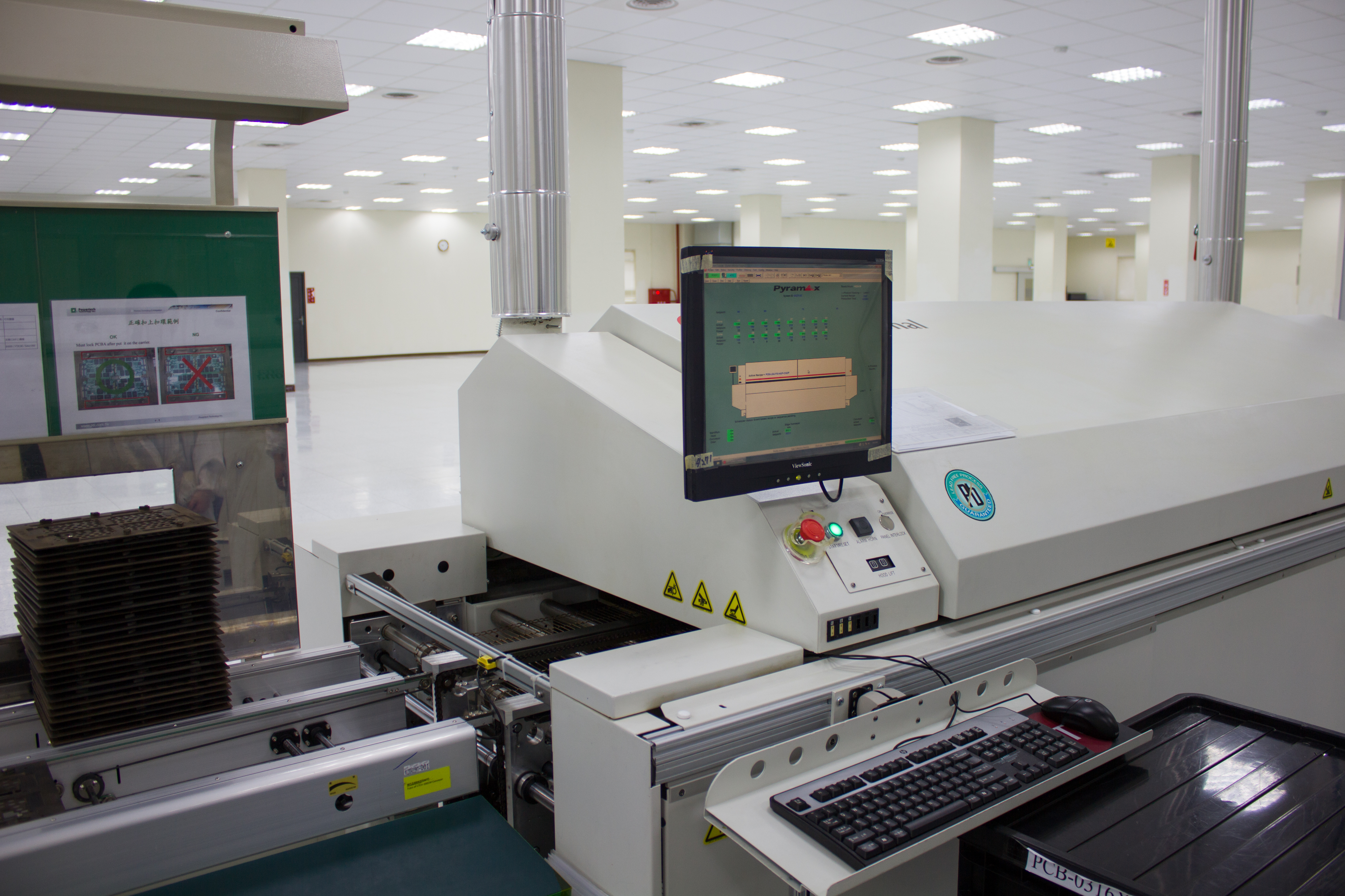
With all the components in place, the drives enters the reflow oven that melts the solder paste and secures electrical connectivity between all chips. The whole reflow process takes about five minutes and the temperature increases gradually at first before dropping quickly in the last stage of the reflow. The exact temperature profile is unique and has been achieved through science, but there's also trial and error in the mix.
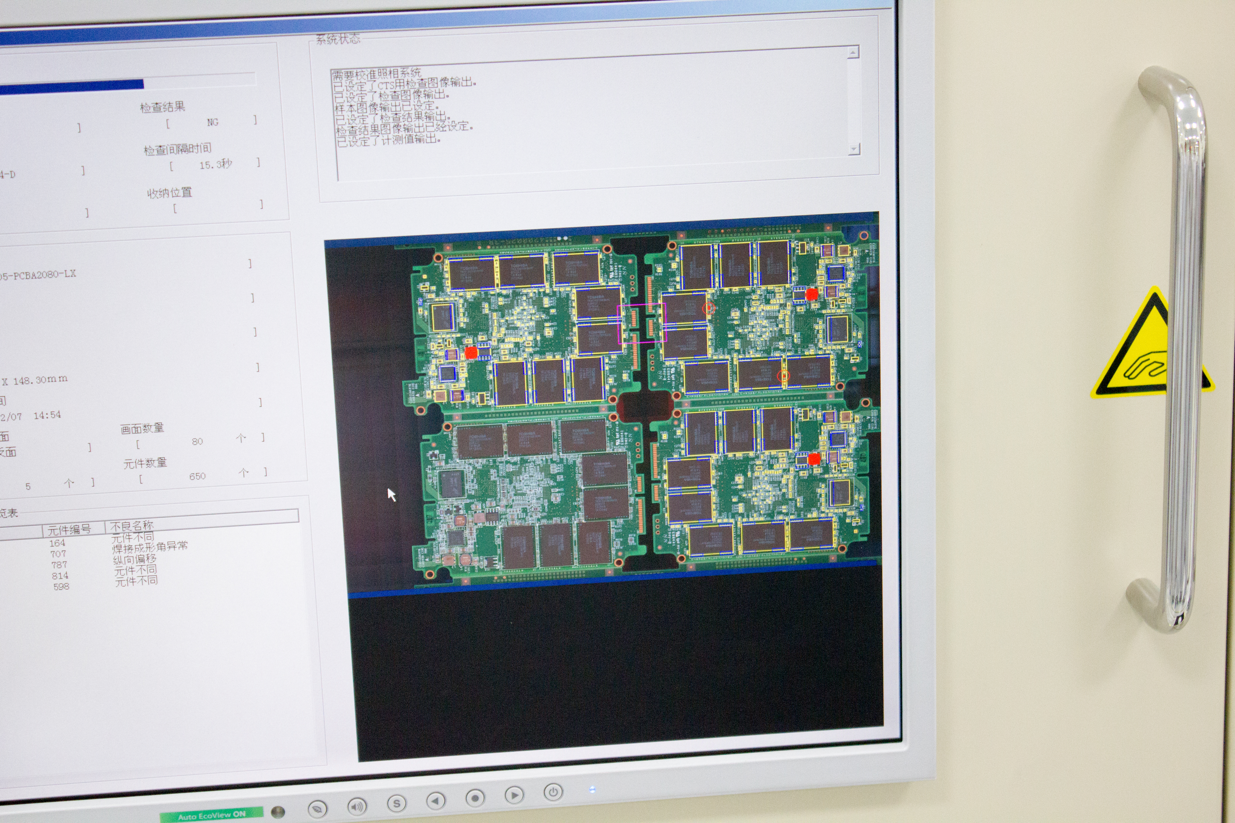
After the reflow the PCBs go through an automatic optical inspection, which compares the produced PCBs against a picture of a perfect PCB to spot any errors (such as misaligned chips and insufficient solders). The automatic inspection is followed by a manual human eye inspection to ensure that all PCBs passing this point should be, at least visually, suitable to go on sale.
For double-sided PCBs, the whole procedure from printing the PCB to visual inspection is then repeated because only one side of the PCB can be worked at a time. That's why many smaller capacity SSDs we see are single-sided because it essentially cuts the PCB assembly steps in half, which reduces cost.
The final step of the PCB assembly is to connect the SATA and power connector, which is separate from the rest of the PCB. I've seen a couple of SSDs where the SATA and power connectors are actually integrated to the PCB, which saves one assembly step, and it's also something that OCZ is considering, but for now the connector remains separate. In M.2 the connector is always a part of the PCB, so from a manufacturing perspective M.2 is slightly more cost efficient than 2.5" drives are.
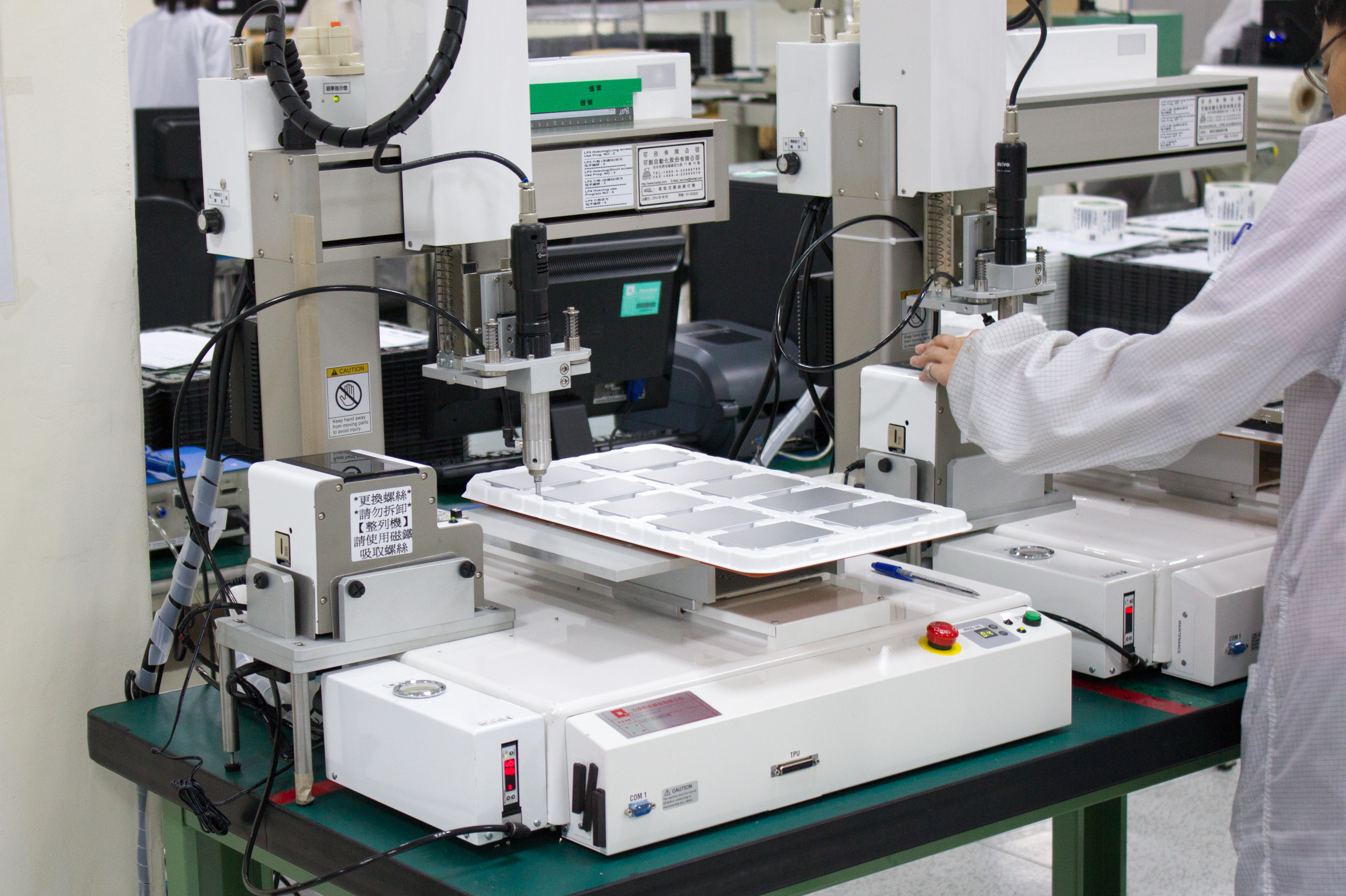
Once the PCB assembly is fully complete, the PCBs are separated and cut from the frame. The PCB is then put inside the final metal chassis and the screws are screwed automatically by the machine above.


64 Comments
View All Comments
dreamslacker - Tuesday, May 26, 2015 - link
Seems like they have to de-panelize the boards before mounting the SATA connector because of the orientation during the panel design (the SATA connector pads are facing each other).JoyTech - Monday, June 1, 2015 - link
Kristian: just curious roughly how many people are employed at the OCZ SSD factory? Maybe it is confidential, but curious as to the number of employees, because you mentioned OCZ looking at automating parts of their process; where the process as of now looks pretty automated, especially for the critical steps.belawrence - Monday, June 1, 2015 - link
For those mentioning "How It's Made", they did an episode showing the manufacturing process of SSDs already - I've seen it at least ten times by now.boe - Monday, June 15, 2015 - link
bring on some 10TB and 32TB 3d NAND drives!