Chipworks Publishes Samsung Galaxy S6 Teardown
by Joshua Ho on April 3, 2015 6:00 PM EST- Posted in
- Smartphones
- Samsung
- Mobile
- Galaxy S6
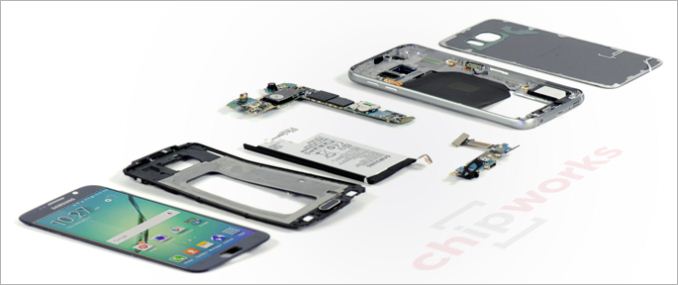
Recently, Chipworks managed to get their hands on the Galaxy S6 and tear down the device to get a closer look at the ICs (integrated circuit) present in the device, which allows for additional analysis of the device. We’re still working on our full review, but we can take a quick look at what Chipworks has found in the device.
This includes an Exynos 7420 SoC that we’ve previously discussed, a Shannon 333 modem along with a Shannon 928 Transceiver and Shannon 710 envelope tracker for the RF front-end. Interestingly, they’ve found an ST-Microelectronics touch controller, which seems to be for the display. Given that most of the Galaxy S and Note family uses Cypress’ CapSense solution for the capacitive touch keys, it’s likely that this is true for the Galaxy S6 as well. Interestingly enough, Chipworks has also identified a Samsung C2N8B6 companion ISP present in the Galaxy S6.

Probably the most interesting aspect of the teardown thus far is that the die size of the 14nm FinFET Exynos 7420 is about 78 mm^2, which is incredibly small compared to the 113 mm^2 size of the 20nm Exynos 5433. It’s unlikely that this is purely due to process as the metal interconnect pitch improvements are relatively minimal when compared to 20nm HKMG, so it’s likely that we’re looking at a great deal of optimization in layout and possibly some IP blocks removed in order to reduce die size. With a die shot floorplan we should be able to figure out exactly what Samsung did to achieve this, and get a good idea of what Samsung has done for the Exynos 7420 which should help with our full review of the Galaxy S6.
Source: Chipworks


47 Comments
View All Comments
FlushedBubblyJock - Friday, April 24, 2015 - link
A friend of mine recently acquired the Moto G - ( cricket ) and it's speakers are tremendously loud, surprisingly loud.I just don't get it how on a PHONE they have lousy speakers when they KNOW hands free is nearly required everywhere now and movies and videos and "driving maps" and so many things require the speaker(s) inherently.
WHAT GIVES HOW ARE THEY SO THICK !?
hung2900 - Friday, April 3, 2015 - link
"so it’s likely that we’re looking at a great deal of optimization in layout and possibly some IP blocks removed in order to reduce die size"I think it's hard to not have a major improvement in this node processing, because the GPU also increase from 6 to 8 cores, which occupy a relatively bigger area.
Gondalf - Saturday, April 4, 2015 - link
Or more likely the not so good 20nm process was underutilized to archieve higher yields. It is a common pratice to stay "large" in not critical layers as there are yields issues.Anyway around 80mm2 is pretty in line with 14/16nm processes density capability. Intel apparently is more dense with Airmont and it's oversized GPU (many say around 50mm2, but is too early to confirm this data).
Gondalf - Saturday, April 4, 2015 - link
No, from Intel datasheet CherryTrail apparently is 71mm2, still the GPU is four time larger than in Baytrail.So both processes are nicely dense in spite of more IP blocks on die.
hung2900 - Saturday, April 4, 2015 - link
You don't get the point. The node 14nm FinFET of Samsung is known as the smaller interconnect but no die shrink (14nm BEOL and 20nm FEOL), and the GPU is still Mali-760 but more cores. Theorically Exynos 7420 is bigger than Exynos 5433 but actually it's much smaller, meaning that there may be an actual die shrink here.Baytrail is processed on Intel's 22nm FinFET (22nm BEOL and 26nm FEOL), while CherryTrail is process on Intek's 14nm FinFET (14nm both BEOL and FEOL). The die shrink is significant here.
Gondalf - Saturday, April 4, 2015 - link
I have got the point, still IMO 5433 was manufactured "large" on 20nm to increase the yields. You know that every process has at least three flavours: maximum density, medium density, fast clock density. Likely Samsung chosen medium density for better yields on 20nm, but this time Sam forced the maximum density on this 14nm SKU; after all 7420 comes later than 5344 and sure Samsung has solved some issues on the metallization stack.Anyway officially Samsung admit some interesting density advantages of 14nm over 20nm (15% in the best case), but definitively not a full node shrink.
Peroxyde - Saturday, April 4, 2015 - link
The LCD display still has the home screen in color on it while it is already completely disassembled. How is it possible?gfieldew - Saturday, April 4, 2015 - link
LCD display? It's an OLED display, unless you accidentally commented in the wrong post or something.BillBear - Saturday, April 4, 2015 - link
Be sure to devote plenty of ink to the S6 #Bendgate problem.https://www.youtube.com/watch?v=3Y7tPczbOec
Solandri - Sunday, April 5, 2015 - link
Even in that video, you can see the iPhone 6 *remains* bent after the load is removed. The S6 reverts back to its original shape.Of course its screen cracked, but they say the screen continued to function and it was only the glass which failed. Which is why flexible OLED screens are going to eventually win out over LCD on phones. The whole bending issue one of the reasons why plastic is a better material for phones than metal, despite the "premium feeling" misnomer held by millions of people who don't know the first thing about materials science. Better to have a phone which bends and reverts back to its original shape, than a phone which bends and stays bent.