The NVIDIA GeForce GTX Titan X Review
by Ryan Smith on March 17, 2015 3:00 PM ESTGM200 - All Graphics, Hold The Double Precision
Before diving into our look at the GTX Titan X itself, I want to spend a bit of time talking about the GM200 GPU. GM200 is a very interesting GPU, and not for the usual reasons. In fact you could say that GM200 is remarkable for just how unremarkable it is.
From a semiconductor manufacturing standpoint we’re still at a standstill on 28nm for at least a little bit longer, pushing 28nm into its 4th year and having all sorts of knock-on effects. We’ve droned on about this for some time now, so we won’t repeat ourselves, but ultimately what it means for consumers is that AMD and NVIDIA have needed to make do with the tools they have, and in lieu of generational jumps in manufacturing have focused on architectural efficiency and wringing out everything they can get out of 28nm.
For NVIDIA those improvements came in the form of the company’s Maxwell architecture, which has made a concentrated effort to focus on energy and architectural efficiency to get the most out of their technology. In assembling GM204 NVIDIA built the true successor to GK104, putting together a pure graphics chip. From a design standpoint NVIDIA spent their energy efficiency gains on growing out GM204’s die size without increasing power, allowing them to go from 294mm2 and 3.5B transistors to 398mm2 and 5.2B transistors. With a larger die and larger transistor budget, NVIDIA was able to greatly increase performance by laying down a larger number of high performance (and relatively larger themselves) Maxwell SMMs.
On the other hand for GM206 and the GTX 960, NVIDIA banked the bulk of their energy savings, building what’s best described as half of a GM204 and leading to a GPU that didn’t offer as huge of a jump in performance from its predecessor (GK106) but also brought power usage down and kept costs in check.
Not Pictured: The 96 FP64 ALUs
But for Big Maxwell, neither option was open to NVIDIA. At 551mm2 GK110 was already a big GPU, so large (33%) increase in die size like with GM204 was not practical. Neither was leaving the die size at roughly the same area and building the Maxwell version of GK110, gaining only limited performance in the process. Instead NVIDIA has taken a 3rd option, and this is what makes GM200 so interesting.
For GM200 NVIDIA’s path of choice has been to divorce graphics from high performance FP64 compute. Big Kepler was a graphics powerhouse in its own right, but it also spent quite a bit of die area on FP64 CUDA cores and some other compute-centric functionality. This allowed NVIDIA to use a single GPU across the entire spectrum – GeForce, Quadro, and Tesla – but it also meant that GK110 was a bit jack-of-all-trades. Consequently when faced with another round of 28nm chips and intent on spending their Maxwell power savings on more graphics resources (ala GM204), NVIDIA built a big graphics GPU. Big Maxwell is not the successor to Big Kepler, but rather it’s a really (really) big version of GM204.
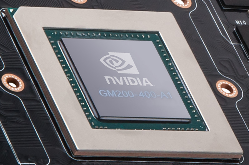
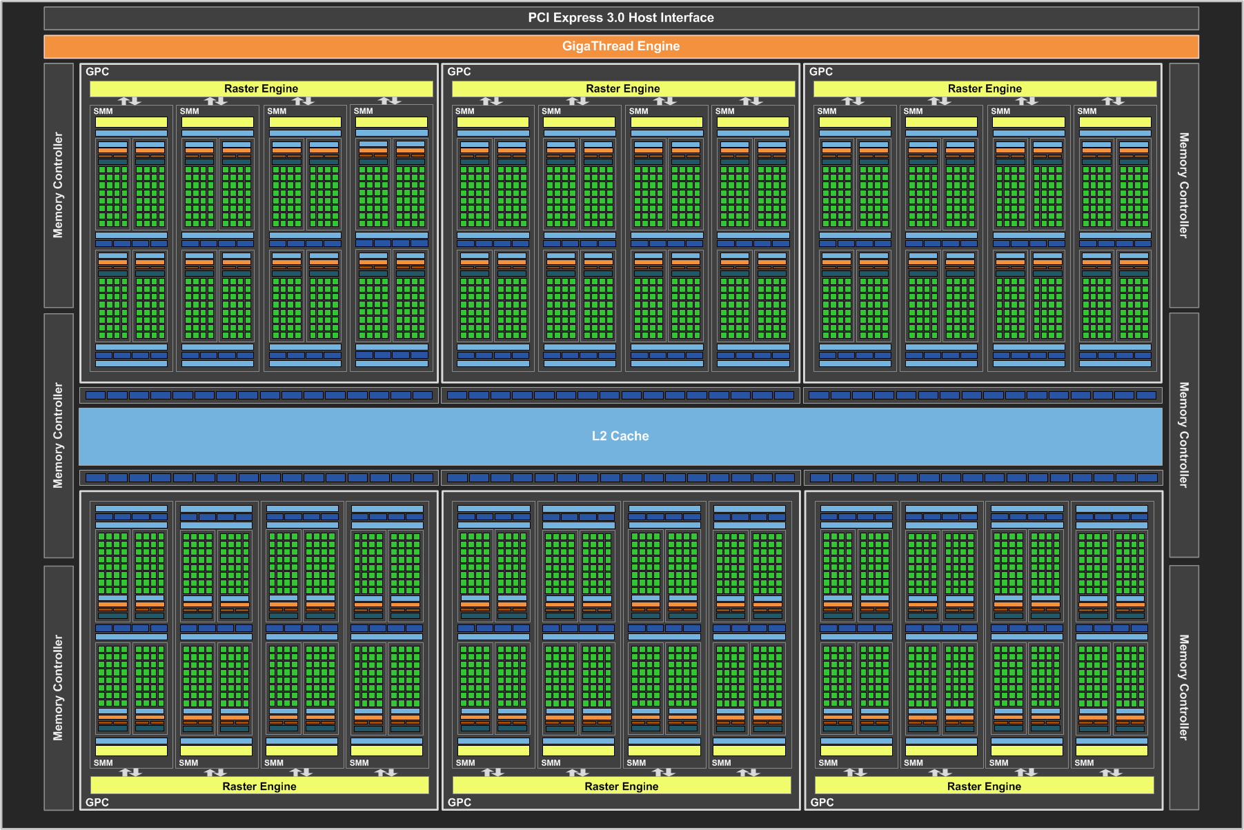
GM200 is 601mm2 of graphics, and this is what makes it remarkable. There are no special compute features here that only Tesla and Quadro users will tap into (save perhaps ECC), rather it really is GM204 with 50% more GPU. This means we’re looking at the same SMMs as on GM204, featuring 128 FP32 CUDA cores per SMM, a 512Kbit register file, and just 4 FP64 ALUs per SMM, leading to a puny native FP64 rate of just 1/32. As a result, all of that space in GK110 occupied by FP64 ALUs and other compute hardware – and NVIDIA won’t reveal quite how much space that was – has been reinvested in FP32 ALUs and other graphics-centric hardware.
| NVIDIA Big GPUs | ||||
| Die Size | Native FP64 Rate | |||
| GM200 (Big Maxwell) | 601mm2 | 1/32 | ||
| GK110 (Big Kepler) | 551mm2 | 1/3 | ||
| GF110 (Big Fermi) | 520mm2 | 1/2 | ||
| GT200 (Big Tesla) | 576mm2 | 1/8 | ||
| G80 | 484mm2 | N/A | ||
It’s this graphics “purification” that has enabled NVIDIA to improve their performance over GK110 by 50% without increasing power consumption and with only a moderate 50mm2 (9%) increase in die size. In fact in putting together GM200, NVIDIA has done something they haven’t done for years. The last flagship GPU from the company to dedicate this little space to FP64 was G80 – heart of the GeForce 8800GTX – which in fact didn’t have any FP64 hardware at all. In other words this is the “purest” flagship graphics GPU in 9 years.
Now to be clear here, when we say GM200 favors graphics we don’t mean exclusively, but rather it favors graphics and its associated FP32 math over FP64 math. GM200 is still a FP32 compute powerhouse, unlike anything else in NVIDIA’s lineup, and we don’t expect it will be matched by anything else from NVIDIA for quite some time. For that reason I wouldn’t be too surprised if we a Tesla card using it aimed at FP32 users such the oil & gas industry – something NVIDIA has done once before with the Tesla K10 – but you won’t be seeing GM200 in the successor to Tesla K40.
This is also why the GTX Titan X is arguably not a prosumer level card like the original GTX Titan. With the GTX Titan NVIDIA shipped it with its full 1/3 rate FP64 enabled, having GTX Titan pull double duty as the company’s consumer graphics flagship while also serving as their entry-level FP64 card. For GTX Titan X however this is not an option since GM200 is not a high performance FP64 GPU, and as a result the card is riding only on its graphics and FP32 compute capabilities. Which for that matter doesn’t mean that NVIDIA won’t also try to pitch it as a high-performance FP32 card for users who don’t need Tesla, but it won’t be the same kind of entry-level compute card like the original GTX Titan was. In other words, GTX Titan X is much more consumer focused than the original GTX Titan.
Tesla K80: The Only GK210 Card
Looking at the broader picture, I’m left to wonder if this is the start of a permanent divorce between graphics/FP32 compute and FP64 compute in the NVIDIA ecosystem. Until recently, NVIDIA has always piggybacked compute on their flagship GPUs as a means of bootstrapping the launch of the Tesla division. By putting compute in their flagship GPU, even if NVIDIA couldn’t sell those GPUs to compute customers they could sell them to GeForce/Quadro graphics customers. This limited the amount of total risk the company faced, as they’d never end up with a bunch of compute GPUs they could never sell.
However in the last 6 months we’ve seen a shift from NVIDIA at both ends of the spectrum. In November we saw the launch of a Tesla K80, a dual-GPU card featuring the GK210 GPU, a reworked version of GK110 that doubled the register file and shared memory sizes for better performance. GK210 would not come to GeForce or Quadro (though in theory it could have), making it the first compute-centric GPU from NVIDIA. And now with the launch of GM200 we have distinct graphics and compute GPUs from NVIDIA.
| NVIDIA GPUs By Compute | |||||
| GM200 | GK210 | GK110B | |||
| Stream Processors | 3072 | 2880 | 2880 | ||
| Memory Bus Width | 384-bit | 384-bit | 384-bit | ||
| Register File Size (Per SM) | 4 x 64KB | 512KB | 256KB | ||
| Shared Memory / L1 Cache (Per SM) |
96KB + 24KB | 128KB | 64KB | ||
| Transistor Count | 8B | 7.1B(?) | 7.1B | ||
| Manufacturing Process | TSMC 28nm | TSMC 28nm | TSMC 28nm | ||
| Architecture | Maxwell | Kepler | Kepler | ||
| Tesla Products | None | K80 | K40 | ||
The remaining question at this point is what happens from here. Was this divorce of compute and graphics a temporary action, the result of being stuck on the 28nm process for another generation? Or was it the first generation in a permanent divorce between graphics and compute, and consequently a divorce between GeForce/Quadro and Tesla? Is NVIDIA finally ready to let Tesla stand on its own?
With Pascal NVIDIA could very well build a jack-of-all-trades style GPU once more. However having already divorced graphics and compute for a generation, merging them again would eat up some of the power and die space benefits from going to 16nm FinFET, power and space that NVIDIA would likely want to invest in greater separate improvements in graphics and compute performance. We’ll see what Pascal brings, but I suspect GM200 is the shape of things to come for GeForce and the GTX Titan lineup.


276 Comments
View All Comments
Kevin G - Tuesday, March 17, 2015 - link
Last I checked, rectal limits are a bit north of 700 mm^2. However, nVidia is already in the crazy realm in terms of economics when it comes to supply/demand/yields/cost. Getting fully functional chips with die sizes over 600 mm^2 isn't easy. Then again, it isn't easy putting down $999 USD for a graphics card.However, harvested parts should be quiet plentiful and the retail price of such a card should be appropriately lower.
Michael Bay - Wednesday, March 18, 2015 - link
>rectal limits are a bit north of 700 mm^2Oh wow.
Kevin G - Wednesday, March 18, 2015 - link
@Michael BayIntel's limit is supposed to be between 750 and 800 mm^2. They have released a 699 mm^2 product commercially (Tukwilla Itanium 2) a few years ago so it can be done.
Michael Bay - Wednesday, March 18, 2015 - link
>rectal limitsD. Lister - Wednesday, March 18, 2015 - link
lolchizow - Tuesday, March 17, 2015 - link
Yes its clear Nvidia had to make sacrifices somewhere to maintain advancements on 28nm and it looks like FP64/DP got the cut. I'm fine with it though, at least on GeForce products I don't want to pay a penny more for non-gaming products, if someone wants dedicated compute, go Tesla/Quadro.Yojimbo - Tuesday, March 17, 2015 - link
Kepler also has dedicated FP64 cores and from what I see in Anandtech articles, those cores are not used for FP32 calculations. How does NVIDIA save power with Maxwell by leaving FP64 cores off the die? The Maxwell GPUs seem to still be FP64 capable with respect to the number of FP64 cores placed on the die. It seems what they save by having less FP64 cores is die space and, as a result, the ability to have more FP32 cores. In other words, I haven't seen any information about Maxwell that leads me to believe they couldn't have added more FP64 cores when designing GM200 to make a GPU with superior double precision performance and inferior single precision performance compared with the configuration they actually chose for GM200. Maybe they just judged single precision performance to be more important to focus on than double precision, with a performance boost for double precision users having to wait until Pascal is released. Perhaps it was a choice between making a modest performance boost for both single and double precision calculations or making a significant performance boost for single precision calculations by forgoing double precision. Maybe they thought the efficiency gain of Maxwell could not carry sales on its own.testbug00 - Tuesday, March 17, 2015 - link
If this is a 250W card using about the same power as the 290x under gaming load, what does that make the 290x?Creig - Tuesday, March 17, 2015 - link
A very good value for the money.shing3232 - Tuesday, March 17, 2015 - link
Agree.