NVIDIA Announces GeForce GTX Titan X
by Ryan Smith on March 4, 2015 1:45 PM EST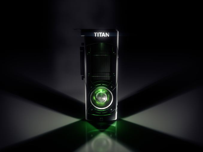
During today’s GDC session on Epic’s Unreal Engine, NVIDIA CEO Jen-Hsun Huang dropped in as a special guest to announce NVIDIA’s next high performance video card, the GeForce GTX Titan X.
In order to capitalize on the large audience of the Unreal session while not spoiling too much ahead of NVIDIA’s own event in 2 weeks – the NVIDIA GPU Technology Conference – NVIDIA is playing coy with details on the product, but they have released a handful of details along with a product image.
| NVIDIA Titan Specification Comparison | |||||
| GTX Titan X | GTX Titan Black | GTX Titan | |||
| Stream Processors | ? | 2880 | 2688 | ||
| Texture Units | ? | 240 | 224 | ||
| ROPs | 96? | 48 | 48 | ||
| Core Clock | ? | 889MHz | 837MHz | ||
| Boost Clock | ? | 980MHz | 876MHz | ||
| Memory Clock | ? | 7GHz GDDR5 | 6GHz GDDR5 | ||
| Memory Bus Width | 384-bit? | 384-bit | 384-bit | ||
| VRAM | 12GB | 6GB | 6GB | ||
| FP64 | ? | 1/3 FP32 | 1/3 FP32 | ||
| TDP | ? | 250W | 250W | ||
| Transistor Count | 8B | 7.1B | 7.1B | ||
| Architecture | Maxwell | Kepler | Kepler | ||
| Manufacturing Process | TSMC 28nm? | TSMC 28nm | TSMC 28nm | ||
| Launch Date | Soon | 2/18/14 | 02/21/13 | ||
| Launch Price | A Large Number | $999 | $999 | ||
The GPU underlying GTX Titan X is 8 billion transistors, which similar to the original GTX Titan’s launch means we’re almost certainly looking at Big Maxwell. NVIDIA will be pairing it with 12GB VRAM – indicating a 384-bit memory bus – and it will once again be using NVIDIA’s excellent metal cooler and shroud, originally introduced on the original GTX Titan.
No further details are being provided at this time, and we’re expecting to hear more about it at GTC. Meanwhile Epic’s master engine programmer Tim Sweeney was gifted the first GTX Titan X card, in recognition of NVIDIA and Epic’s long development partnership and the fact that Epic guys are always looking for more powerful video cards to push the envelope on Unreal Engine 4.


104 Comments
View All Comments
hammer256 - Wednesday, March 4, 2015 - link
Well, there's only so much efficiency and computation magic you can get out at the same node, so I guess we are pretty stuck until that shrink then :( Maybe next year?dragonsqrrl - Wednesday, March 4, 2015 - link
It isn't certain yet. In fact recent rumors have pointed to 20nm for Fiji XT, and some have argued that TSMC's 20nm process, despite being optimized for low power, is still perfectly capable of achieving AMD's clockspeed targets. We'll see, but I would be surprised if Fiji XT is even feasible on 28nm if the rumored specs are true.MrSpadge - Wednesday, March 4, 2015 - link
Hitting AMDs frequency targets is not so hard when you consider they're running Tonga on R9 285 at 925 MHz. And this is not even using low voltage.hammer256 - Wednesday, March 4, 2015 - link
I'm guessing the yield for 20nm is not too insane for large chips, after all Apple's chip is like 3B transistors. Would be cool if AMD does use 20nm. At least keep things fresh and interesting.RussianSensation - Friday, March 6, 2015 - link
Most rumours state the opposite that R9 300 series will be exclusively on 28nm. 20nm at TSMC is for SoCs and is unlikely to be suitable for flagship performance GPUs.MrSpadge - Wednesday, March 4, 2015 - link
With 12 GB VRAM in the top model the 384 bit bus is practically certain. From this they can go to 6 GB at full performance. Anything else will be slower after a certain amount of RAM is used up. So you probably rather want a 6 GB GTX980Ti at full performance than an 8 GB version with a handicap.CiccioB - Wednesday, March 4, 2015 - link
I think many of you have not understood that it is still better having 8GB as 6GB full speed +2GB slow speed than simply having 6GB full speed.Also the GTX970 may have 0.5GB slow memory partition, but this is still faster than system memory, so it is better to have it than not. People believing that the card would be better with 3.5GB or VRAM simply do not understand how things work.
MrCommunistGen - Wednesday, March 4, 2015 - link
This was the behavior I inferred from reading the article as well, with the additional constraint that even if you have a high memory bandwidth platform (like Haswell-E), access to main memory is still bottlenecked by a PCI-E 3.0 x16 bus to significantly less than the 0.5GB "slow" partition. I'm assuming that there are significant latency costs associated with reaching out to main memory compared to the local "slow" partition as well, although those are harder to quantify.Refuge - Monday, March 9, 2015 - link
It is correct, it is slower than the bulk of the Vram, but still much faster than accessing anything anywhere else in the system.Those that bitch about the performance can just go in a hole and not come out, because it was a great card for the $$$ when it came out, and guess what? It still is!
Those that are upset about the failure to properly advertise it at all, and instead the insistance that it has the "Same memory structure as the GTX 980" have a valid claim, even if it really is just a chance to try and get something for free, I would jump on too! :P
Oxford Guy - Wednesday, March 4, 2015 - link
Right, because it's advantageous to have XOR contention and 28 gb/s bandwidth that causes microstutter and slows the performance of the fast VRAM.