ARM Announces Cortex-A72, CCI-500, and Mali-T880
by Andrei Frumusanu on February 3, 2015 5:30 PM EST- Posted in
- Smartphones
- Arm
- Mobile
- Mali
- Cortex A72
- CCI-500
- Mali T880
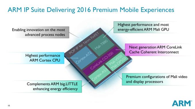
Today ARM is announcing three brand-new premium IP designs targeted at high-end mobile SoCs. We're still only starting to get widespread commercial availability of ARM's latest generation of SoCs, which includes the Cortex-A57 in big.LITTLE configuration coupled with the A53 as little cores, and the newest T760 Mali GPUs. But, while those designs are still ramping up through offerings from Samsung, Qualcomm, HiSilicon and co. this year, ARM isn't staying still and already looking forward to 2016 and beyond.
Cortex-A72 - a new high end core
At the center of today's announcements a new high-end performance core which succeeds the A57 in flagship devices. ARM was very vague about the architectural characteristics of the new design, disclosing for now only estimates of the chip's performance and power targets. ARM promises a 3.5x sustained performance increase over the A15 generation of SoCs while remaining in the same power budget. One has to note that we're talking about performance targets on TSMC's 16nm FinFET+ node versus previous nodes such as 28 and 20nm, which in itself should bring large clock and power advantages.

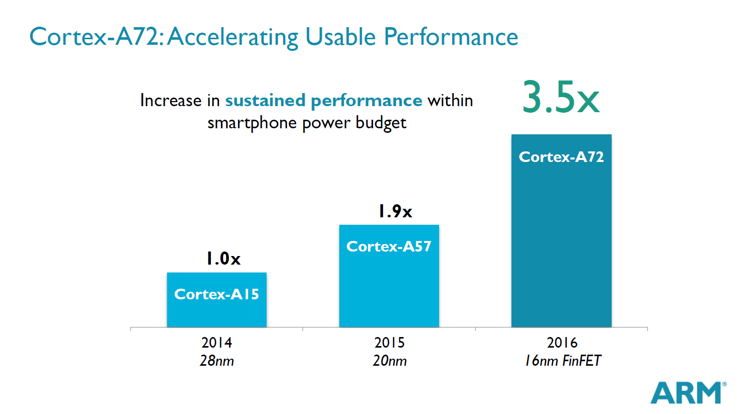
The A72 targets roughly 1.9X the sustained performance of current 20nm A57 SoCs, meaning the Exynos 5433 and the Snapdragon 810 can be taken as the base for comparisons. ARM doesn't yet mention peak performance so we may be talking about overall power efficiency gains that enable future SoCs to throttle much less. ARM will be divulging more information on the architecture of the A72 in the coming months, and we're hoping to have a better picture on the actual IPC and efficiency gains of the new flagship core by then.
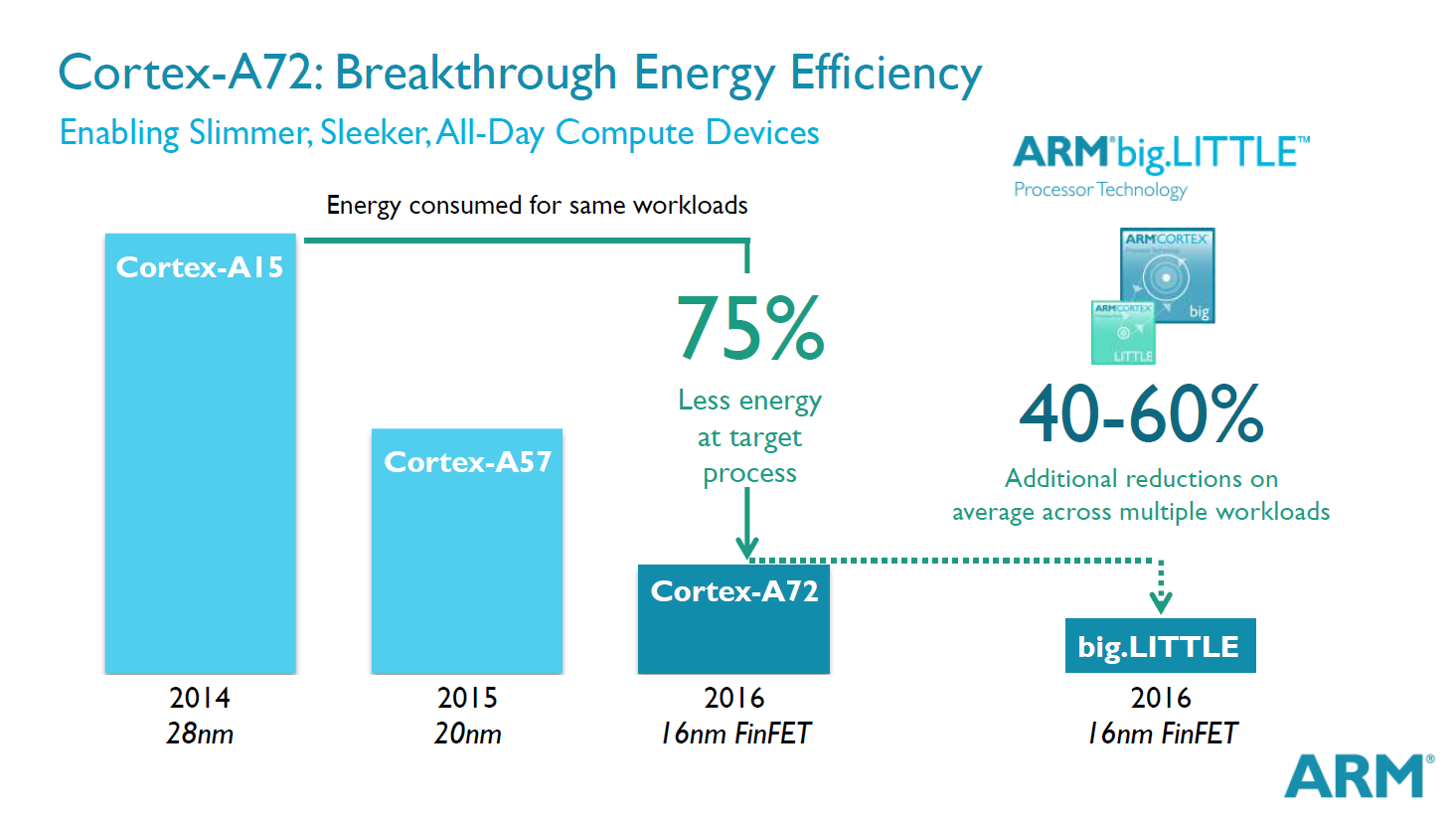
The Cortex-A72, being a "big" core, can be partnered up with the already existing A53 LITTLE core architectures. ARM has said in the past that the A53 took in-order designs to new heights, and while work on a successor is underway, it seems that for now we'll be sticking with the A53 architecture for a while longer.
HiSilicon, MediaTek and Rockchip are listed among more than then launch partners which have already licensed the Cortex-A72 processor, so expect to see a variety of vendors offering the new ARM IP in 2016.
CoreLink CCI-500 SoC interconnect
It's been over 3 years since ARM initially announced their CCI-400 (Cache Coherent Interconnect), which saw widespread usage as the corner-stone technology enabling big.LITTLE heterogeneous multiprocessing in all consumer SoCs from the Exynos 5410 to the latest Snapdragon 810. While ARM also offered high-end alternatives such as the CCN-5XX (Cache Coherent Network) range of interconnects, these were targeted more at server-applications and not meant for mobile SoCs in smartphones or tablets.
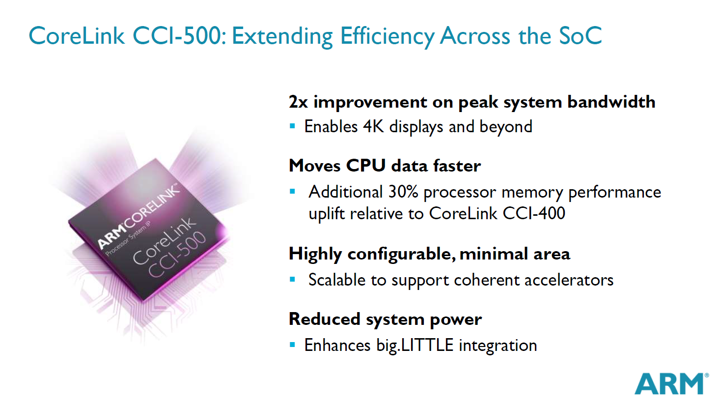
The CCI-500 is a large upgrade over the CCI-400 as it introduces a variety of new functionality over its predecessor. The largest change in functionality is the addition of a snoop filter on the interconnect itself. Until now snoop control was only possible between CPUs within a single cluster. The addition of a snoop filter on the interconnect allows for power efficiency benefits as the amount of transactions when doing cache lookups is decreased, enabling both reduced overhead on the interconnect and also higher idle residency times on the CPU cores. This reduced overhead also frees up memory bandwidth on the interconnect, and ARM claims this enables for 30% better memory performance on the CPU ports.
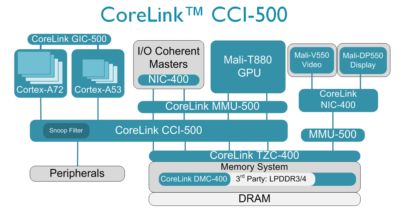
The new interconnect also doubles up on its system bandwidth: We now have twice the number of ACE (AXI Coherency Extension) ports, enabling usage of a maximum of four CPU clusters (instead of the two that are possible with the CCI-400). We'll be continuing to see the usage of only two clusters in mobile designs, but the new IP gives licensees the flexibility to deviate according to their needs.
The increased bandwidth and numbers of ports on the interconnect also opens up the possibility of quad-channel memory controllers, resulting in 128-bit memory buses. The Snapdragon 805 was the first mobile product to feature such capability, although Qualcomm used a non-cache-coherent interconnect in their design.
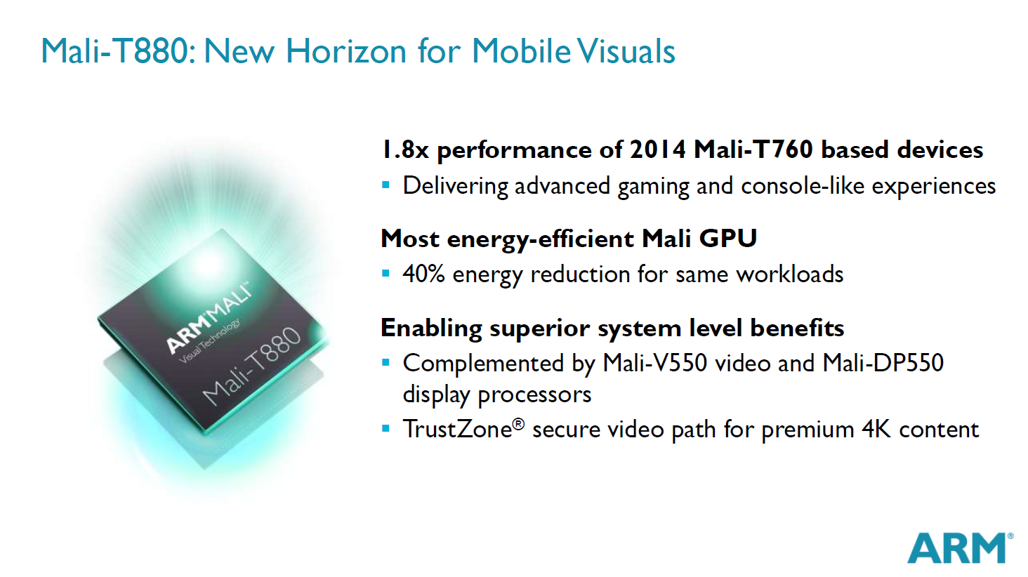
Mali T880 GPU
Lastly, ARM also announced a new member of the T800 series of Mali GPUs. In addition to the T820, T830 and T860 comes the T880. ARM was again light on details of what this new configuration brings, only promising a 1.8x increase performance over 2014 Mali T760 GPUs and a 40% reduction in energy consumption for the same workloads.
With today's announcements, ARM appears to be addressing its weaknesses in mobile SoCs by focusing on sustained performance and efficiency of its big core architecture. We also have the much needed upgrade in the memory/interconnect subsystem and an expansion in its GPU IP offering.
Source: ARM


49 Comments
View All Comments
name99 - Wednesday, February 4, 2015 - link
You have explained why more than 2 large cores is frequently unnecessary. No-one is denying that.What you haven't justified is why the background work demands 4 small cores rather than just 1.
UpSpin - Wednesday, February 4, 2015 - link
" Fully custom ARM SoC's like apple's a8, are engineered around power efficiency at all workloads."Sure, so what must have been the reason for Apple to include an Cortex M3 core in their A7/A8 SoC. I mean, there should be no reason, if the A7/A8 is so highly efficient both in low power and high power modes. Yet, it isn't. Apple quietly added a companion core for sensor data processing.
With big.LITTLE, there's no need for this. The main CPU can do all this, using a low power CPU. Additionally it can do much more.
You can make the main cores as efficient as possible, but you'll never be able to make them as efficient as dedicated cores, which are trimmed for power efficiency and most importantly, are build using power efficient transistors, instead of performance transistors.
extide - Wednesday, February 4, 2015 - link
Even big.LITTLE could use something like a Cortex M3/M4 -- they are SIGNIFICANTLY less power than even an A53 or A7 or even A5 !extide - Wednesday, February 4, 2015 - link
(As a sensor fusion hub, I mean)V900 - Thursday, February 5, 2015 - link
That's nonsense. Show me a phone that uses an A53 core to do the kind of tasks you use an M3 core for, and I'll show you a phone that was designed by somebody without a degree, and which lasts for two hours on a full charge.You'd see a CortexM companion core used alongside big.Little impkementations, because using anything else than an M core for simple tasks like counting steps, etc.would be a colossal waste.
Companion cores like the Cortex M class cores are puny compared to A53 or even A7 or A5 cores. A-class cores are easily ten(s) times more powerful. But also use ten(s) times the power.
M-class cores are designed to last for months on a single charge. The smaller ones like the M3 are more of a microcontroller than a microprocessor.
jjj - Tuesday, February 3, 2015 - link
Eager to see some realistic perf numbers, not sure why they chose to go with a very creative math, just undermines their credibility and that's hard to regain. Does it beat Denver or Denver on 16ff+ or Core M , hopefully we find out soon. The guys with custom cores (AMD included) might be not too happy about this, depending on how their own core does.There is a typo in the article, "instead of ten partners" it says "then partners".
azazel1024 - Wednesday, February 4, 2015 - link
Agreed. If you note, that is a 75% increase in efficiency for similar workloads...comparing an A15 on 28nm versus 16nm FINFET...that process and technology difference alone probably more than accounts for a 75% difference in efficiency! That is two full nodes, plus planar to FINFET!!!!Sounds like something that'll be that much more heavily throttled if they try to fit it in to a smart phone. Now, burst performance is nice, but when you start getting in to only a few seconds of burst performance, and then throttling 40-60%+ it provides speed ups to fewer and fewer tasks.
Granted, the efficiency advantages means higher sustained workload speeds...but the process changes alone probably should provide that, the new architecture sounds like it likely will only provide a minor boost, very minor, accept in thermally unconstrained installations or for very short periods of time until throttled. Core is getting closer to ARM power levels and ARM is getting closer to Core power levels.
No free lunch.
hahmed330 - Tuesday, February 3, 2015 - link
Boring... Accept the processor A72..psychobriggsy - Wednesday, February 4, 2015 - link
"Except".And one of ARM's weaknesses has been memory efficiency, so the new interconnect will surely improve matters there.
I'm looking forward to more details, sadly ARM's product releases are very different from Intel's and AMD's, as they license designs rather than sell product. At least they have completed the 16nm POP hard macros though, so it will be easy to incorporate into a design (I'm sure that SoC designers have designs already just waiting for the final cores to slot in).
name99 - Wednesday, February 4, 2015 - link
The interconnect is a lot more interesting than you seem to think.Intel uses a ring (multiple rings on high-end Xeons) rather than a crossbar (even on Xeon Phi, which seems a bizarre choice).
For ARM to use a crossbar (with the extra silicon that implies compared to a ring) suggests that they are really striving for high performance interCPU communication (and probably that they have a goal of, in the nearish future) switching to multiple large L3 cache slices along with NUCA and all that implies.