NVIDIA Launches Tesla K80, GK210 GPU
by Ryan Smith on November 17, 2014 9:30 AM EST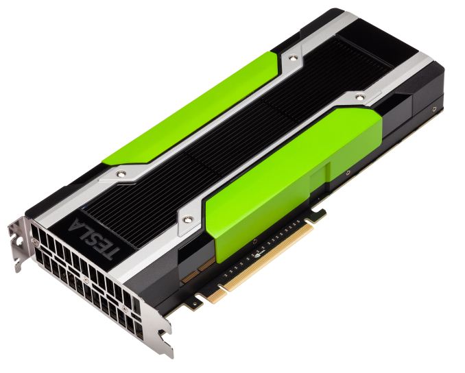
Kicking off today is the annual International Conference for High Performance Computing, Networking, Storage, and Analysis, better known as SC. For NVIDIA, next to their annual GPU Technology Conference, SC is their second biggest GPU compute conference, and is typically the venue for NVIDIA’s summer/fall announcements. Earlier we covered the announcement of NVIDIA’s role in the US Department of Energy’s latest supercomputer acquisitions, and today we’ll be taking a look at NVIDIA’s latest Tesla GPU compute card, Tesla K80.
At SC’13 NVIDIA introduced the Tesla K40, the first “fully enabled” Kepler Tesla card. Based on the GK110B variant of NVIDA’s GPU, this was the first Tesla product to ship with all 2880 CUDA cores enabled. Typically one would think that with a fully enabled GK110 based board that the Kepler Tesla lineup would have reached its apex, but for SC’14 NVIDIA will be pushing the performance envelope a bit harder in order to produce their fastest (and densest) Tesla card yet.
| NVIDIA Tesla Family Specification Comparison | ||||||
| Tesla K80 | Tesla K40 | Tesla K20X | Tesla K20 | |||
| Stream Processors | 2 x 2496 | 2880 | 2688 | 2496 | ||
| Core Clock | 562MHz | 745MHz | 732MHz | 706MHz | ||
| Boost Clock(s) | 875MHz | 810MHz, 875MHz | N/A | N/A | ||
| Memory Clock | 5GHz GDDR5 | 6GHz GDDR5 | 5.2GHz GDDR5 | 5.2GHz GDDR5 | ||
| Memory Bus Width | 2 x 384-bit | 384-bit | 384-bit | 320-bit | ||
| VRAM | 2 x 12GB | 12GB | 6GB | 5GB | ||
| Single Precision | 8.74 TFLOPS | 4.29 TFLOPS | 3.95 TFLOPS | 3.52 TFLOPS | ||
| Double Precision | 2.91 TFLOPS (1/3) | 1.43 TFLOPS (1/3) | 1.31 TFLOPS (1/3) | 1.17 TFLOPS (1/3) | ||
| Transistor Count | 2 x 7.1B(?) | 7.1B | 7.1B | 7.1B | ||
| TDP | 300W | 235W | 235W | 225W | ||
| Cooling | Passive | Active/Passive | Passive | Active/Passive | ||
| Manufacturing Process | TSMC 28nm | TSMC 28nm | TSMC 28nm | TSMC 28nm | ||
| Architecture | Kepler | Kepler | Kepler | Kepler | ||
| Launch Price | $5000 | $5499 | ~$3799 | ~$3299 | ||
Dubbed the Tesla K80, NVIDIA’s latest Tesla card is an unusual and unexpected entry into the Tesla lineup. For Tesla K80 NVIDIA has produced a new GPU – GK210 – and then put two of them into a single card. The net result is a card with no peers; NVIDIA has done dual GPU Tesla cards before (Tesla K10) and there have been dual GPU GK110 cards before (GeForce Titan Z), but nothing quite like Tesla K80.
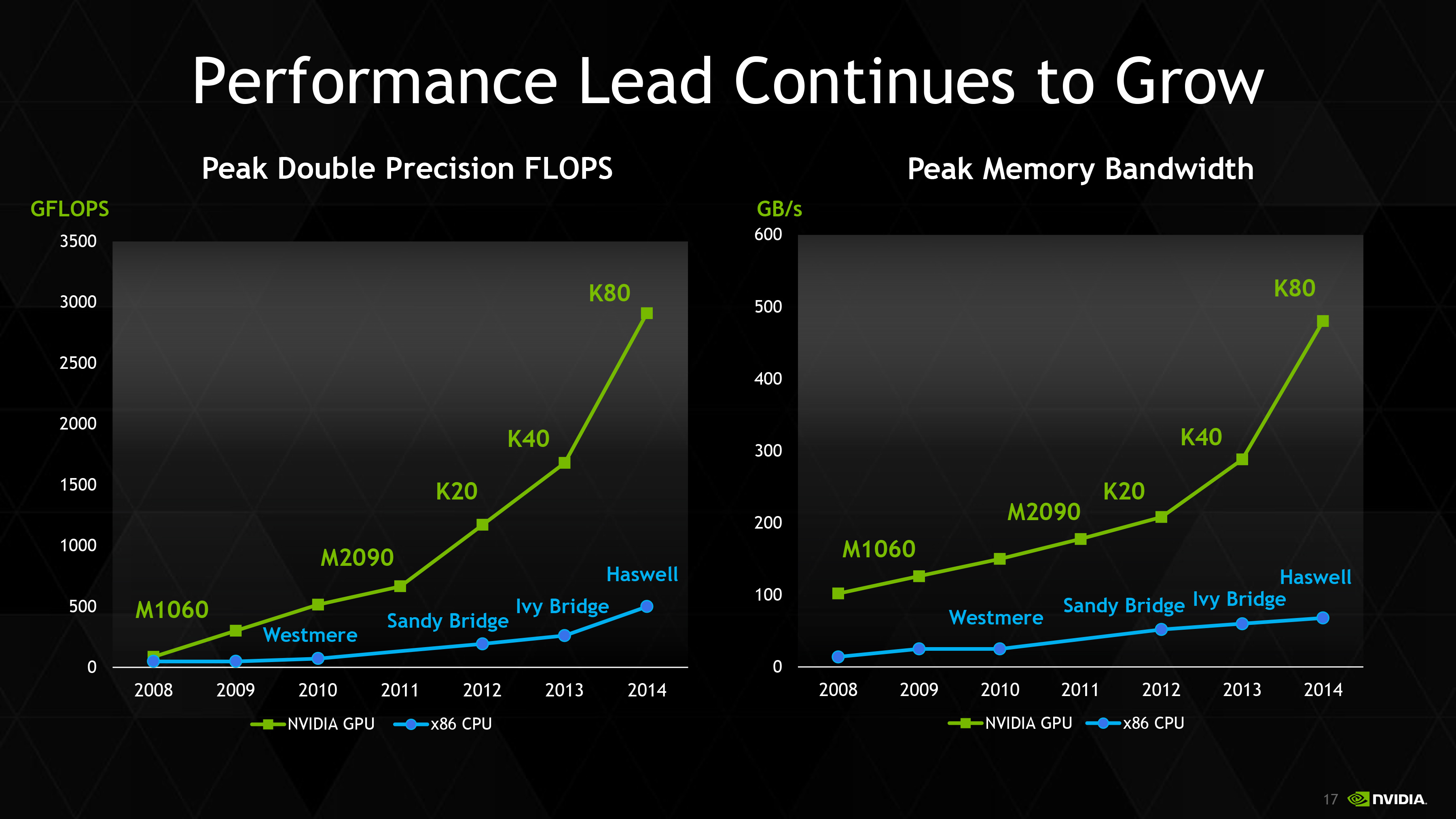
From both a performance and power standpoint, NVIDIA is expecting to once again raise the bar. Factoring in GPU Boost (more on that later), Tesla K80 is rated for a maximum double precision (FP64) throughput of 2.9 TFLOPS, or a single precision (FP32) throughput of 8.7 TFLOPS. Compared to Tesla K40 this is roughly 74% faster than NVIDIA’s previous top-tier Tesla card, though GPU Boost means that the real performance advantage will not reach quite that high.
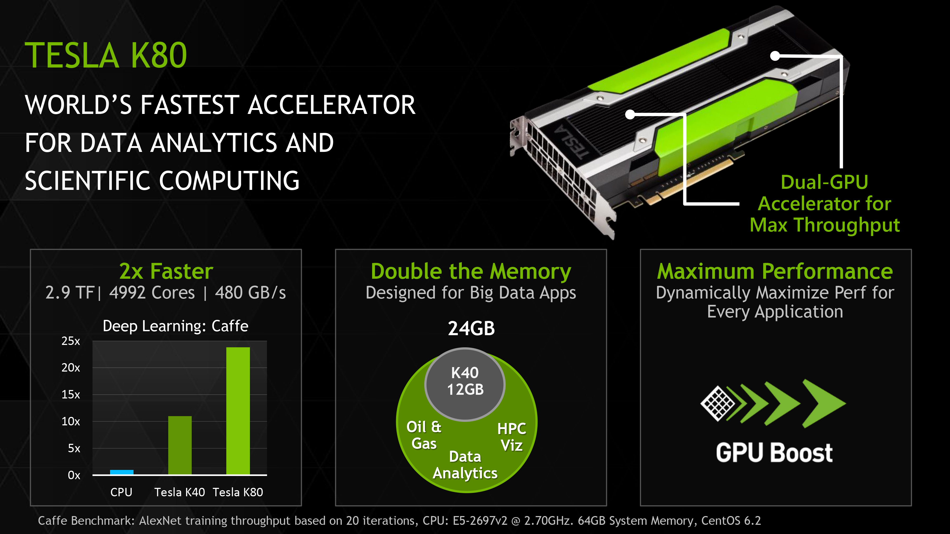
Fitting a pair of GPUs on a single card is not easy, and that is especially the case when those GPUs are GK210. Unsurprisingly then, NVIDIA is shipping K80 with only 13 of 15 SMXes enabled on each GPU, for a combined total of 4,992 CUDA cores enabled. This puts the clockspeed at a range of 562MHz to 870MHz. Meanwhile the memory clockspeeds have also been turned down slightly from Tesla K40; for Tesla K80 each GPU is paired with 12GB of GDDR5 clocked at 5GHz, for 240GB/sec of memory bandwidth per GPU. This puts the total memory pool between the two GPUs at 24GB, with 480GB/sec of bandwidth among them.
Meanwhile Tesla K80 will also be pushing the power envelope, again to get 2 GPUs on a single card. Whereas Tesla K40 and K20X were 235W cards, Tesla K80 is a 300W card. The fact that NVIDIA was able to get two high performance GPUs within 300W is no small achievement in and of itself, though for this reason GPU Boost plays a big part in making the overall product viable. Consequently energy efficiency gains are almost entirely reliant on what kind of performance Tesla K80 can sustain at 300W; the worst case scenario is that it’s only 2% more energy efficient than K40 while the best case is 59%, with the realistic case being somewhere in the middle.
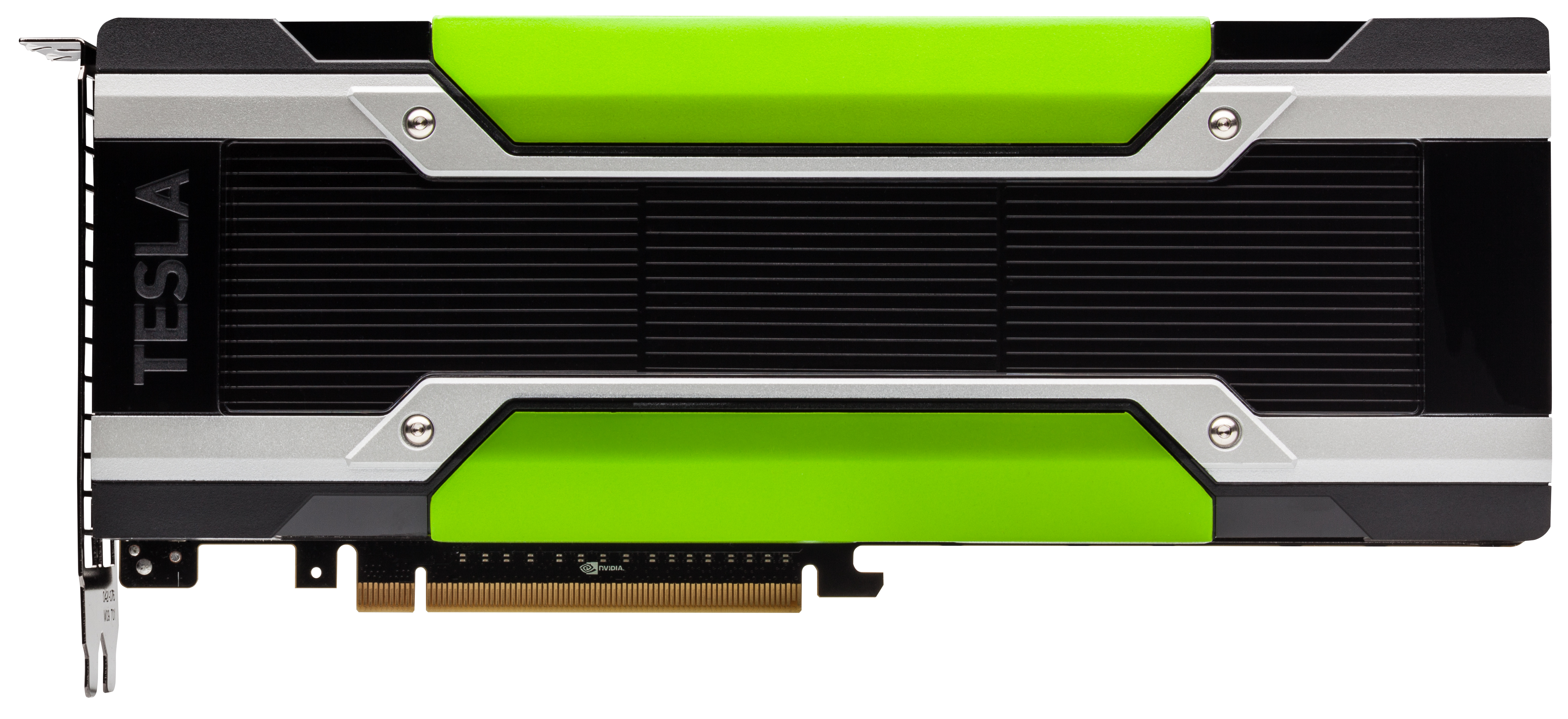
Speaking of efficiency, for Tesla K80 NVIDIA has crammed it into a standard size double-slot Tesla card enclosure, so on a volume basis Tesla K80 packs quite a bit more power per slot than K40, improving NVIDIA’s space efficiency. So far we have only seen passive cards, and given the need to move 300W of heat we expect that these cards will need to be passive in order to be paired up with appropriately powerful external fans.

Moving on, let’s start with GK210. Introduced with Tesla K80, GK210 is fundamentally the 3rd revision of GK110, following in the footsteps of GK110B, introduced on Tesla K40. Compared to GK110B, which was really just a cleanup of GK110, GK210 is a more radical alteration of GK110. This time around NVIDIA has made some real feature changes that although maintain GK210’s lineage from GK110, none the less make it meaningfully different from its predecessor.
| GK110 Family GPUs | |||||
| GK210 | GK110B | GK110 | |||
| Stream Processors | 2880 | 2880 | 2880 | ||
| Memory Bus Width | 384-bit | 384-bit | 384-bit | ||
| Register File Size | 512KB | 256KB | 256KB | ||
| Shared Memory / L1 Cache |
128KB | 64KB | 64KB | ||
| Transistor Count | 7.1B(?) | 7.1B | 7.1B | ||
| Manufacturing Process | TSMC 28nm | TSMC 28nm | TSMC 28nm | ||
| Architecture | Kepler | Kepler | Kepler | ||
| Tesla Products | K80 | K40 | K20/K20X | ||
To that end, while NVIDIA hasn’t made any sweeping changes such as adjusting the number of CUDA cores or their organization (this is still a GK110 derivative, after all) NVIDIA has adjusted the memory subsystem in each SMX. Whereas a GK110(B) SMX has a 256KB register file and 64KB of shared memory, GK210 doubles that to a 512KB register file and 128KB of shared memory. Though small, this change improves the data throughput within an SMX, serving to improve efficiency and keep the CUDA cores working more often. NVIDIA has never made a change mid-stream like this to a GPU before, so this marks the first time we’ve seen a GPU altered in a later revision in this fashion. That said, this also reflects on the state of the GPU market, and how Kepler will still be with us for some time to come.

Overall I suspect that along with the memory change, NVIDIA has used this latest revision to once again tighten up the design of their HPC GPU to correct errata and reduce power consumption (thereby improving performance), which is part of the reason that NVIDIA is able to get two of these GPUs in a 300W card. Meanwhile GK210 will be in an odd place as it will likely be the first NVIDIA GPU not to end up in a consumer card; prior to this generation every GPU has pulled double duty as both a compute powerhouse and a graphics king. But with GM204 clearly ahead of GK110/GK210 in graphics, GK210 seems destined to Tesla cards and at most a Titan card for the budget compute market. Given the costs in bringing a new GPU revision to market – just the masks alone are increasingly expensive – the situation implies that NVIDIA expects to more than make back their money on additional sales enabled by GK210, which in turn indicates that they have quite a bit of faith in the state of the GPU compute market since it alone would be where the additional revenue would come from.
The final piece of the puzzle for Tesla K80 is GPU Boost. In the Tesla space NVIDIA introduced this on Tesla K40 in a far more limited implementation than on their consumer GPUs. Tesla K40 had to obey its TDP, but operators could select which of 3 clockspeeds they wanted, picking the one that comes closest to (but not exceeding) TDP for the best performance. However with Tesla K80 NVIDIA has now implemented a full and dynamic GPU boost implementation; just as in their consumer cards, the card will clock itself as high as the TDP will allow.
The change in implementation is no doubt driven by the more complex thermal environment of a multi-GPU card, not to mention the need to squeeze out yet more efficiency. As with consumer cards TDP headroom left on the table is potential performance wasted, and for Tesla this is no different. Without GPU boost and building to a worst case scenario, K80 would not be much more efficient than K40, as evidenced by the 562MHz core clockspeed. That said, with K40 NVIDIA made clockspeeds deterministic for GPU workload sync issues, so it’s not entirely clear why non-deterministic clockspeeds are now okay just a year later.
Specifications aside, Tesla K80 represents an unexpected evolution in Tesla designs. Strictly speaking, Tesla K80 is often but not always superior to Tesla K40. Per GPU throughput is lower than on Tesla K40, so given a task that doesn’t scale well over multiple GPUs a Tesla K40 could still be faster. None the less, the majority of tasks Tesla cards will run will cleanly scale well over multiple GPUs – this being a cornerstone of the modern HPC paradigm of clusters of processors – so outside of a few edge cases K80 should be faster, generally quite a bit faster.
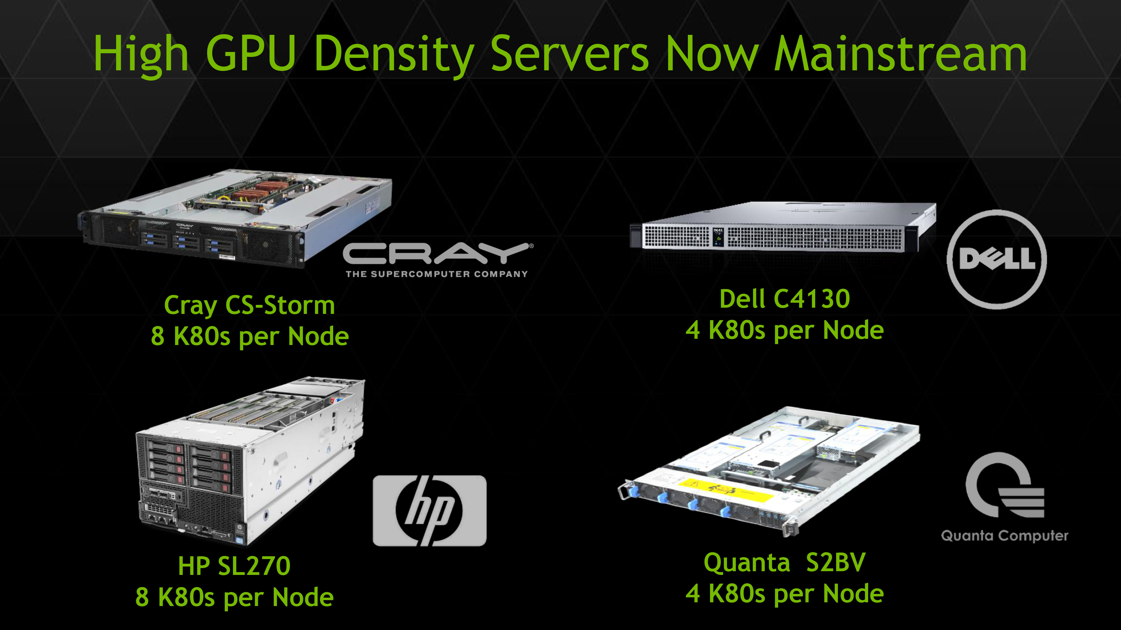
Otherwise the density implications are quite interesting. A 300W TDP presents its own challenges, but in surmounting that it’s now possible to get 8 GK210 GPUs in a 1U form factor, which would put the FP64 compute throughput of such a setup at over 10 TFLOPS in 1U.
Wrapping things up, Tesla K80 will be a hard launch from NVIDIA and their partners, with individual cards and OEM systems equipped with them expected to be available today. Officially NVIIDA does not publish MSRPs for Tesla cards, but the first listings are already up. It looks like Tesla K80 is rolling out at $5000, which is actually a bit cheaper than the $5500 K40 first launched at (and now sells for $3900).


28 Comments
View All Comments
Ryan Smith - Monday, November 17, 2014 - link
Whoops. Thanks.Kevin G - Monday, November 17, 2014 - link
I'm really curious what the die size is on GK210. The GK110B is 550 mm^2 already. The larger register and L1 caches are just going to push it close to 600 mm^2.I also think we'll see a Tesla K30 and K50 at some point using binned versions of these chips. The K50 would be fully enabled at higher clock speeds than the K40 and the K30 carrying a configuration and clock speed in between the K40 and K20X. I'd also expect a Quadro refresh to start utilizing this new chip as well (K6200).
This also means that the big Maxwell chip, GM110/210 is clearly going to be a 2015 product. GK210 is just a stop gap solution until they're ready.
Mushkins - Monday, November 17, 2014 - link
I feel like it's about time the industry came up with a more accurate term for these cards. GPU is a little disingenuous as they're not being used to process graphics at all in this implementation, it's all compute performance for data crunching regardless of what the chip was originally designed to do.TiGr1982 - Monday, November 17, 2014 - link
Two suggestions:1) Use GPGPU instead
2) Understand GPU as "General Processing Unit" in this context (though it's still confusing; not a good idea probably)
So, this is still Kepler-based accelerator, even for the $$$$ (which it will certainly have) or even $$$$$ price, which simply means there is no "big Maxwell" aka GM200 in a few months ahead, at least - because in the past (2 years ago), if I'm not mistaken, the first implementation of Kepler GK110 "big Kepler" aka GK110 happened to be Tesla K20X shipped for (still 2nd in top500) "Titan" supercomputer (not to be confused with "Titan" graphics cards).
RussianSensation - Monday, November 17, 2014 - link
There appears to be an inconsistency in the specs for K40. The K80 part is listed as more than > 2x as fast in SP and DP performance over K40. The Boost Clock is used for K80 to arrive at its performance data but for K40 the Base/Core Clock is used. It should really be:K40 @ 810mhz = 4.67 Tflops SP, 1.56 Tflops FP-64 / DP
K40 @ 875mhz = 5.04 Tflops SP, 1.68 Tflops FP-64 / DP
Otherwise, it seems only fair to use the Core Clock of the K80 too instead of its Boost Clock.
Interesting how K80 isn't a full fledged Titan Z Tesla derivative.
darckhart - Monday, November 17, 2014 - link
Something's not right with the tables. In one, the K80 is listed as 2x 2496, and the paragraph says based on GK210. In another table, the GK210 is listed with 2880 cores. Also, I am assuming it's still 1/3 double precision?Ryan Smith - Monday, November 17, 2014 - link
The tables are correct. The GPUs used in K80 do not ship with all CUDA cores enabled, likely for power reasons.CiccioB - Tuesday, November 18, 2014 - link
I doubt that. It is more efficient to use more silicon at lower frequency to get the same performances (yet it costs more doing that).I think the disabled cores are for yield. I doubt that a monster bigger than 7bilions of transistor that occupies about 600mm^2 has an high yield. They are just using the best they can (and make user pay for that).
Seen that on gaming cards GK110 has been replaced by GM204 and that on Tesla GK110 has been replaced by this GK210, I think nvidia has stopped making the GK110 completely. It is possible that it was not that profitable (mainly on gaming cards). If this is true we'll soon see a new Quadro using this chip as well.
SirKnobsworth - Monday, November 17, 2014 - link
Passive cooling? I'm guessing this is intended for a server chassis with strong directional airflow?Ryan Smith - Monday, November 17, 2014 - link
Correct.