ARM A53/A57/T760 investigated - Samsung Galaxy Note 4 Exynos Review
by Andrei Frumusanu & Ryan Smith on February 10, 2015 7:30 AM ESTCortex A57 - Architecture
Shifting gears to a look at the Exynos 5433’s high-performance CPU cores, we have the Cortex-A57, the successor to ARM's earlier ARMv7 Cortex-A15.
As ARM’s first high-performance ARMv8 core, A57 is jumping into an interesting market. A57’s first year is likely to be even more successful than A15 was, and yet this is going to be the most competitive landscape yet within the ARM ecosystem, thanks to a larger number of ARM architecture licensees than ever before. Many of these licensees are in the server realm – companies like AppliedMicro who are making a run at the server market – meanwhile others such as Apple and NVIDIA have used their designs in the consumer market, even beating out A57 by nearly a year in the case of Apple. Still, within the narrower confines of the Android space, A57 is currently the CPU to beat for 2015, with everyone from Samsung to Qualcomm licensing the design for their high-end CPUs.
Diving into A57 itself then, A57 is in many ways a direct evolution and continuation of the A15 design. Intended for 28nm and newer nodes, A57 essentially picks up where A15 left off, introducing ARMv8 support while further ramping up ARM's IPC, overall single-threaded performance, and even energy efficiency. Under the hood ARM has made a number of changes to improve efficiency while retaining other elements of A15 that still make sense. The end result is something akin to an Intel “tock”, meaning we’re looking at something that isn’t a massive overhaul of the architecture (e.g. Cyclone or Denver) but institutes a number of new features and optimizations.
A57 is at its heart a fully out-of-order design, making for a very interesting contrast to NVIDIA’s Denver, which we took a look at last week. This basically being the norm to NVIDIA’s unorthodoxy, A57 is a much more traditional CPU design that follows ARM’s historical design tendencies and is similarly intended to fit in roughly the same design envelope as A15.
From a high-level perspective, ARM makes a fairly straightforward tradeoff in terms of performance and power consumption. A57 is designed to be bigger and more performant than A15, but in turn it can consume more power as well. ARM’s internal projections for A57 are that it can achieve 25-50% better IPC at a cost of 20% higher power consumption if built on the 28nm node. In terms of overall energy efficiency this should leave A57 with a decent edge over A15, thanks to performance increases outpacing the power consumption increase.
The wildcard factor in all of this will be the manufacturing node, especially the temperamental 20nm processes. While A57 can be produced on 28nm, in keeping with the pace of manufacturing technology and the need to offset its larger size, the first consumer A57 designs like the Exynos 5433 are being produced at 20nm, as opposed to 28nm for the bulk of A15 designs. The smaller process helps to keep the size of A57 relatively small – enough to easily fit four cores on an SoC – and it means that we’re getting the power efficiency gains that come from a smaller process node, adding to A57’s architectural gains. However it also means that the performance gains on shipping A57 SoCs are going to be influenced by manufacturing factors such as leakage and the viability of higher clock speeds, so the real-world performance gains over A15 are going to be a bit more variable. Overall ARM is pushing for a higher IPC design in part to better control these factors, as higher IPC designs would allow for partners to ramp down the clock speeds a bit, and thereby voltage and power consumption.
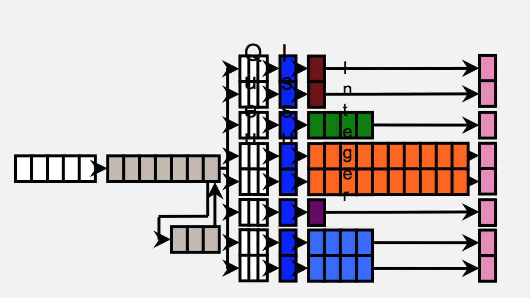
In any case, let’s talk about the design of the A57. In creating the A57, ARM tells us that their goal was to design the CPU around the kinds of compute workloads they expect to see over the next few years, in order to get the best real-world performance out of their design. To that end, ARM says that in planning A57 they found that mobile workloads aren’t as instruction pipeline sensitive as they once were, and as a result the biggest bottlenecks aren’t in the pipeline itself but rather in feeding the pipeline. Consequently, A57’s design has made fewer changes to the A15 pipeline and focused more on improving the hardware supporting the pipeline, such as fetch, decode, and out-of-order execution capabilities.
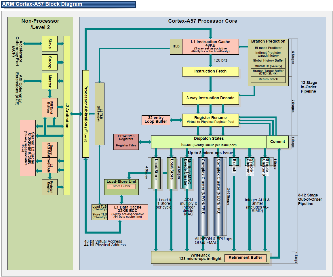
Image courtesy of Hiroshige Goto
Starting at the front then, at the fetch stage ARM has made numerous small changes. The L1 cache has been expanded from 32KB in A15 to 48KB in A57, and similarly its associativity has gone from 2-way to 3-way. The overall increase in cache helps to improve performance, though perhaps more importantly the larger instruction cache helps to offset the larger size of the 64-bit ARM instructions. Meanwhile the Branch Target Buffer, used to store past branches and better predict future branches, has seen its size doubled entirely, now coming in at 2K-4K. Meanwhile on the data side the L1 data cache is left unchanged at 32KB.
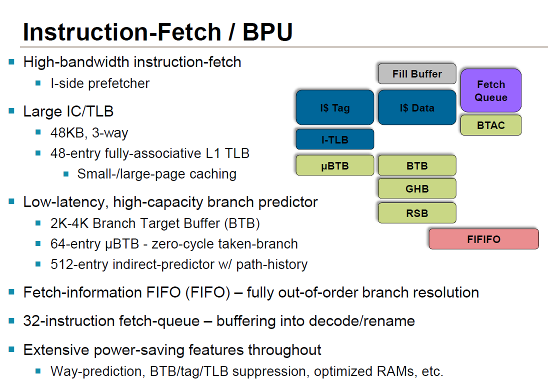
L2 cache on the other hand is configurable on a per-SoC basis. A57 supports L2 cache sizes between 512KB and 2MB, with the cache being 16-way set-associative. Each A57 core gets its own interface to the L2 cache, so there is no bandwidth sharing at the interface level. It also bears mentioning at this point that with A57 ARM now supports multiple memory page sizes on top of the standard 4K memory page size, though the larger pages are primarily for server use.
For instruction decoding, A57 retains the familiar 3-wide decoder front-end. ARM always faces a fine balancing act on decoder size – wider decoders are physically larger – and as with A57 this falls in line with ARM’s goal to focus on feeding the pipeline as opposed to the pipeline itself, as ARM believes they are not yet at the limit of a 3-wide pathway. Though not wider, the decoder has seen other changes to improve performance and power efficiency. Of particular note, the various decode planes for each instruction set – Thumb, NEON, AArch64, and ARMv7 – can now be power gated so that only the decode plane necessary is powered up, helping to offset the cost of needing to support four different instruction formats. Register renaming has also been tweaked at the decode stage, particularly to take advantage of the fact that ARMv8 allows for a flat register map, as opposed to the earlier banked register map.
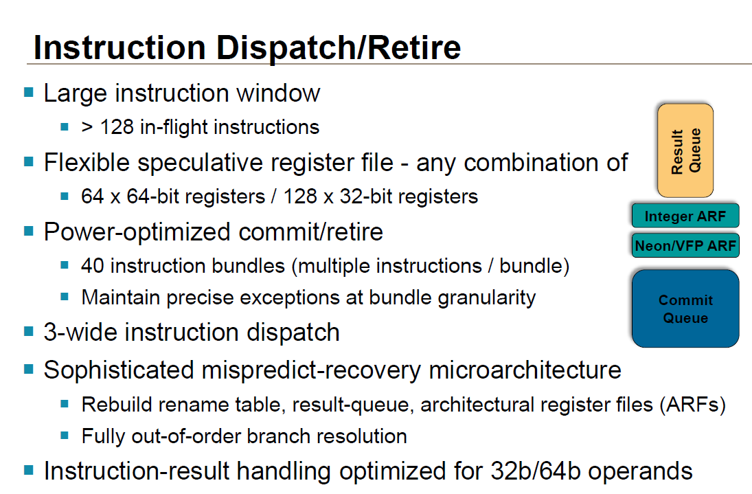
Meanwhile ARM has also made a few important changes at the instruction dispatch and execution stage. Of note, the instruction window for OoOE has once again been increased in size; ARM still isn’t commenting on the precise size, but it is said to be able to hold more than 128 instructions to further improve OoOE performance. Elsewhere the register file has been given its own enhancements, primarily for AArch64 compatibility. Each 4K segment of the register file can now be configured as 128 32-bit registers or 64 64-bit registers, allowing for relatively small portions of the file to be switched over to 64-bit mode and avoiding wasting space on values that don’t require the larger register format.
| ARM CPU Core Comparison | ||||||
| Cortex-A15 | Cortex-A57 | |||||
| ARM ISA | ARMv7 (32-bit) | ARMv8 (32/64-bit) | ||||
| Decoder Width | 3 micro-ops | 3 micro-ops | ||||
| Pipeline Length | 18 stages | 18 stages | ||||
| Branch Mispredict Penalty | 15 cycles | 15 cycles? | ||||
| Integer Add | 2 | 2 | ||||
| Integer Mul | 1 | 1 | ||||
| Load/Store Units | 1 + 1 (Dedicated L/S) | 1 + 1 (Dedicated L/S) | ||||
| Branch Units | 1 | 1 | ||||
| FP/NEON ALUs | 2x64-bit | 2x128-bit | ||||
| L1 Cache | 32KB I$ + 32KB D$ | 48KB I$ + 32KB D$ | ||||
| L2 Cache | 512KB - 4MB | 512KB - 2MB | ||||
As for the pipeline itself, both the integer and floating point units have seen some upgrades for performance and 64-bit compatibility reasons. Though ARM doesn’t go into great detail on how they have this arranged, they have integer datapaths for both 32-bit and 64-bit execution, allowing them to only fire up the 64-bit path when they need it. Additional paths do create some complexity, but the pay-off over a single 64-bit path is that additional transistors are not fired up and additional power burnt just to run 32-bit code.
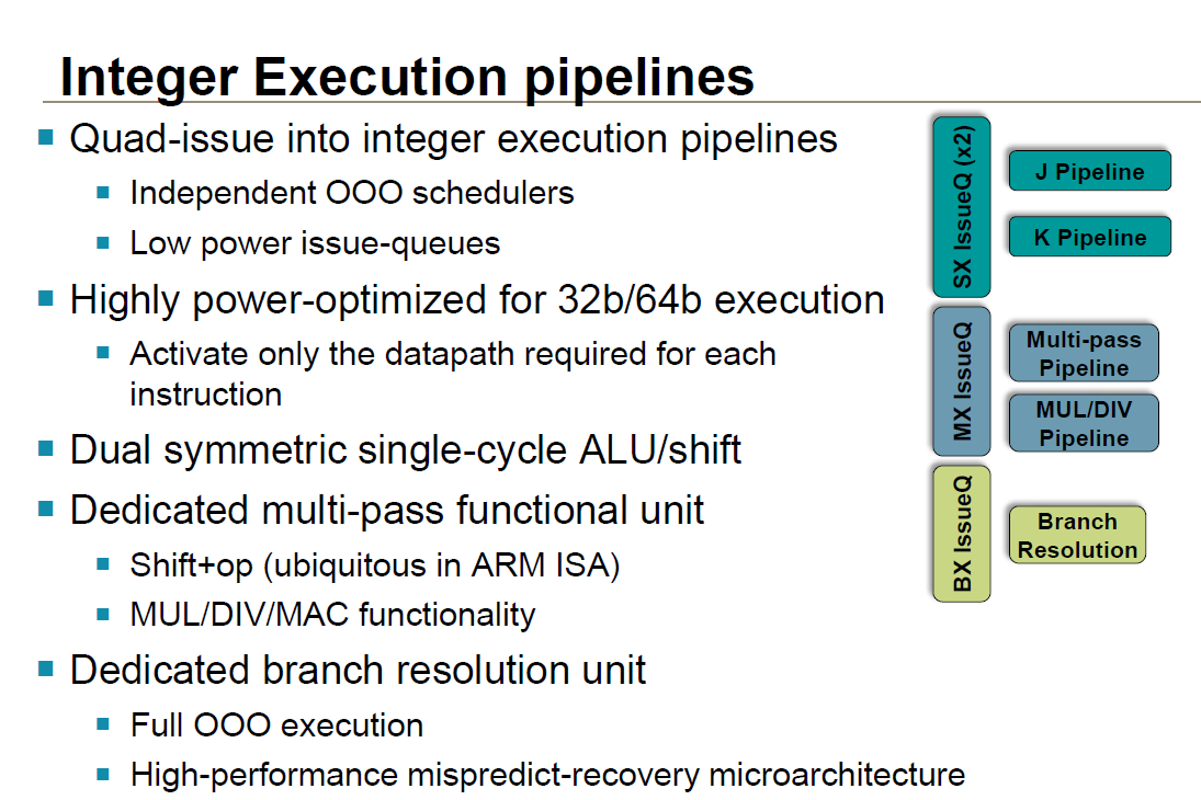
The floating point/NEON units on the other hand are outright wider, doubling from 64-bits to 128-bits and in turn potentially doubling NEON performance (when the FP units can be fully fed). Unlike the integer pipeline there aren’t separate paths for different data sizes, but ARM does tell us that they have worked in some further power optimizations to keep power usage down. These units are now also IEEE-754-2008 compliant when executing ARMv8 code. For the consumer market this does not have much of an impact, but it is an important distinction for the server market, which is another area ARM is hoping to get the A57 into now that they have 64-bit addressing capabilities. Finally, A57 supports an optional cryptography accelerator unit at this stage to speed up AES and SHA1/SHA2-256 performance.

Last but certainly not least, the load/store units have learned a few new tricks as well. Loads can now bypass non-disambiguated stores, which is good for around another 5% increase in performance. At the same time a dependence predictor is now in place at this stage, primarily to help improve OoOE performance by preventing A57 from over-speculating and otherwise harming performance during speculative memory operations.
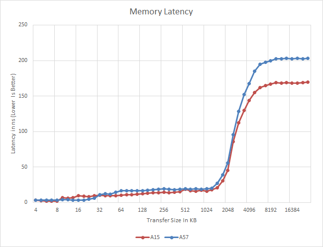
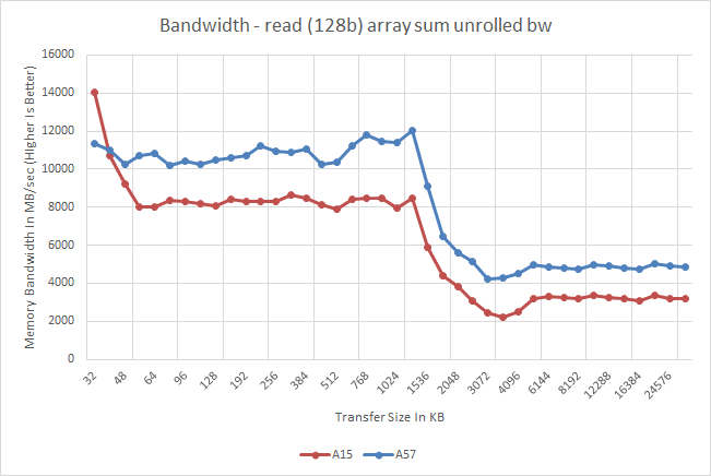
Meanwhile a quick look at memory latency and bandwidth on the A57 cores in the Exynos 5433 finds an unexpected pairing. Latency is virtually unchanged from the A15 through the L2 cache, but once it hits main memory the latency increases by nearly 40ns. On the other hand memory bandwidth is consistently better on the A57, even in cache. As far as latency is concerned this may be due to a Samsung design decision in the SoC itself. Meanwhile the improved bandwidth is likely a consequence of A57's various enhancements to improve throughput within the CPU cores.
ARM's relatively poor memory bandwidth figures have garnered them a poor reputation when it comes to memory performance, but what we are seeing here might be a gross misrepresentation of real-world performance. To understand how these figures come to be, we need to look at how the CPU is wired to the SoC's interconnect and memory controllers. ARM, as opposed to designs by Apple or NVIDIA, uses separate read and write data-ports in its fabric. On the cluster level, this is a dual 128-bit interface (one for reads, one for writes) that connects to matching ports of the SoC's memory controllers via the CCI's (Cache Coherent Interconnect) crossbar architecture. On the Exynos 5430 and 5433, the CCI runs at half the DRAM frequency, meaning 412.5 MHz for the aforementioned SoCs. This results in a maximum physical bandwidth of 6.6 GB/s in each direction.
What most of today's synthetic benchmarks portray is only the bandwidth measured in either direction, giving ARM a distinctive disadvantage. Total achievable bandwidth can reach double these figures. In fact, when we execute simultaneous read and write tests (multithreaded on two CPUs) we benchmark bandwidth numbers reaching the theoretical peaks of the memory controllers at 13.2GB/s. Interestingly, it seems ARM is employing the same setup to the L2 cache as bandwidth there also doubles to up to 25GB/s for the 5430's A15 and 27.5GB/s for the 5433's A57 clusters.
As to why ARM prefers this kind of configuration is a good question. We suspect that there may be power or latency advantages to the design, but we cannot be certain of it. Overall, it should have less of an impact in real-world scenarios as the benchmarks would lead one believe. Use cases where computations are either read or write heavy should only appear in scenarios such as video encoding or texture decompression such as loading video game assets, with the the former not being a real issue in the mobile space due to fixed-function hardware dedicated to the task.
Overall then, as put together A57 serves as the natural step up from A15, both in terms of the underlying design and of the overarching architecture. There is no single great change to drive performance here – and in fact the instruction pipeline isn’t much different in execution – but by focusing on building out for AArch64 execution and improvements to better feed those pipelines, ARM expects that they can get a significant IPC increase over A15. Coupled with 20nm and later 16nm/14nm processes ARM and their partners are hoping to push A57 far, though given the fact that A15 was already a bit power hungry in phones, it will be interesting to see how much of those process gains are spent on performance (clock speeds) and how much is spent on bringing down power consumption.
Meanwhile, ARM’s long-term plans for A57 also call for it to lead a double-life as a server CPU. With a 64-bit memory space, applications running on the A57 can finally address all the memory they need (and then some), so coupled with the IPC increase ARM is hoping to crack the server market in a way that early A15 efforts never did. Among the first companies shipping a server CPU will be AMD and their A1100, so it will be interesting to see how A57 plays out in the server market over the coming year.


135 Comments
View All Comments
toyotabedzrock - Tuesday, February 10, 2015 - link
Dropping the browser tests is just stupid squared and wastes the opportunity to have Google and arm fix the inconsistency issue!Also your performance table for the a57 has an error for the PNG Comp ST.
toyotabedzrock - Tuesday, February 10, 2015 - link
To me it is clear why arm has a new core coming. The a57 was not designed to do 64bit well. If the system uses only 64bit apps it might get bottlenecked.lopri - Tuesday, February 10, 2015 - link
(pg. 6)BaseMark OS II Energy Efficiency test makes no sense to me. I get that perf/watt factor looks worse on the 5433, but why does the test consume more energy when run on big cores only, compared to when run on all 8 cores?
You have explained the performance degration part, but I am not sure whether you mentioned the reduced energy consumption part running 8 cores compared to 4 (big) cores. Running on 8 cores consume a little more than running on 4 LITTLE cores.
I wonder if that benchmark is trust-worthy?
Gigaplex - Tuesday, February 10, 2015 - link
Read through it again. They do comment on that and claim that the switching between big and little cores is likely adding so much overhead they're better off just staying on the big cores.Gigaplex - Tuesday, February 10, 2015 - link
If only there was an edit option... My original comment referred to reduced perf/watt in "8 core" mode rather than just the energy consumption.As to why running on all 8 uses less than only the big 4? It doesn't use them simultaneously, it can only use the big or the little, and it switches between them dynamically. Since the big cores get to idle/sleep when it's running on the little cores, it uses less power overall. This is the whole point of the big.LITTLE design. It's just a shame it doesn't actually work from a performance point of view.
lopri - Tuesday, February 10, 2015 - link
So that means the benchmark is limited to 4-threads, I assume? Stating that would have helped me understand it.Andrei Frumusanu - Wednesday, February 11, 2015 - link
I explained the nature of the XML test and that it was 3 threads:"The test is a good candidate because it offers a scaling load with three threads that put both a high load on some cores and let others exercise their power management states at the same time, definitely behavior you would see in day-to-day applications."
MikhailT - Tuesday, February 10, 2015 - link
Is it me, or does anybody else wish ARM would change their naming scheme?This single quote took 4-5 re-reads for me:
"As far as performance goes, ARM tells us that A53 can match A9 in performance at equivalent clock speeds. Given just how fast A9 is and just how small A53 is, to be able to match A9’s performance while undercutting it in die size and power consumption in this manner would be a feather in ARM’s cap, and an impressive follow-up to the A8-like performance of A7."
lopri - Tuesday, February 10, 2015 - link
Is the "special" frequency only available to ALU-heavy loads on Exynos really a special case? I noticed a similar behavior on S800, too. Adreno 320 should do max 450 MHz, but 99% of the time I see it maxes at 320 MHz. I thought something must be wrong at first, but when I ran benchmarks or other compute-heavy demos, it finally showed me 450 MHz. (not talking about cheating, obviously) It seems like a wide-spread practice.zodiacfml - Tuesday, February 10, 2015 - link
Not surprising outcome. All they need is produce this chip for the sheer number of cores which is popular in some but large markets. The chip is supposed to be good for better efficiency but we didn't see that.