The Google Nexus 9 Review
by Joshua Ho & Ryan Smith on February 4, 2015 8:00 AM EST- Posted in
- Tablets
- HTC
- Project Denver
- Android
- Mobile
- NVIDIA
- Nexus 9
- Lollipop
- Android 5.0
Designing Denver
Diving into the depths of Denver, Denver is in a lot of ways exactly the kind of CPU you’d expect a GPU company to build. NVIDIA’s traditional engineering specialty is in building wide arrays of simple in-order processors, a scheme that maps well to the ridiculously parallel nature of graphics. Whether intentional to tap their existing expertise or just a result of their plan to go in such a divergent route from “traditional” CPUs, Denver makes you stop and ponder GPUs for a moment when looking at its execution workflow.
The results of NVIDIA’s labors in designing Denver has been a wide but in-order processor. With the potential to retire up to 7 operations per cycle, Denver measured front-to-back is wider than A15/A57 and wider than Cyclone. Officially NVIDIA calls this a “7+” IPC architecture, alluding to Denver’s binary translation and code optimization step, and the potential to merge operations as part of the process.
Meanwhile the existence of this code optimizer is the first sign we see that Denver is not a traditional CPU by the standards of ARM/Apple or Intel/AMD. To understand why that is we must first discuss Out of Order Execution (OoOE), why it exists, and why Denver doesn’t have it.
In traditional CPU designs, we make a distinction between in-order designs and out-of-order designs. As appropriately named, in-order designs will execute instructions in the order they receive them, and meanwhile out-of-order designs have the ability to rearrange instructions within a limited window, so long as the altered order doesn’t change the results. For the kinds of tasks that CPUs work with, OoOE improves throughput, but it does come at a cost.
Overall OoOE is considered the next logical step after in-order execution has reached its natural limits. Superscalar in-order execution can potentially scale up to a few instructions at once, but actually achieving that is rare, even with the help of good compilers. At some point other constraints such as memory accesses prevent an instruction from executing, holding up the entire program. In practice once you need performance exceeding a traditional in-order design, then you switch to out-of-order. With OoOE then it becomes possible to scale performance out further, with the ability to use the reodering process to fill wider processors and to keep from losing performance due to stalls.

K1-64 Die Shot Mock-up (NVIDIA)
The cost of OoOE is complexity, die size, and power consumption. The engines to enable OoOE can be quite large, being tasked with queuing instructions, identifying which instructions can be reordered, and ensuring instructions are safe to execute out-of-order. Similarly, there is a power cost to these engines, and that means adding OoOE to a processor can make it much larger and more power hungry, even without actually adding further units for the OoOE engines to fill. Make no mistake, the benefits of OoOE are quite large, but then so is the cost of implementing it.
As such, while OoOE has been treated as the next step after in-order processors it is not the only solution to the problem being pursued. The fundamental problems in-order processors face are a combination of hardware and software; hardware issues such as memory stalls, and software issues such as poor instruction ordering. It stands to reason then that if the performance scaling problem can be solved in hardware with OoOE, then can it be solved in software as well? It’s this school of thought that NVIDIA is pursuing in Denver.
Perhaps the critical point in understanding Denver then is that it is non-traditional for a high-performance CPU due to its lack of OoOE hardware, and for that reason it’s a CPU unlike any of its contemporaries. We’ll get back to the software aspects of Denver in a bit, but for now it’s enough to understand why NVIDIA has not pursued an OoOE design and what they have pursued instead.
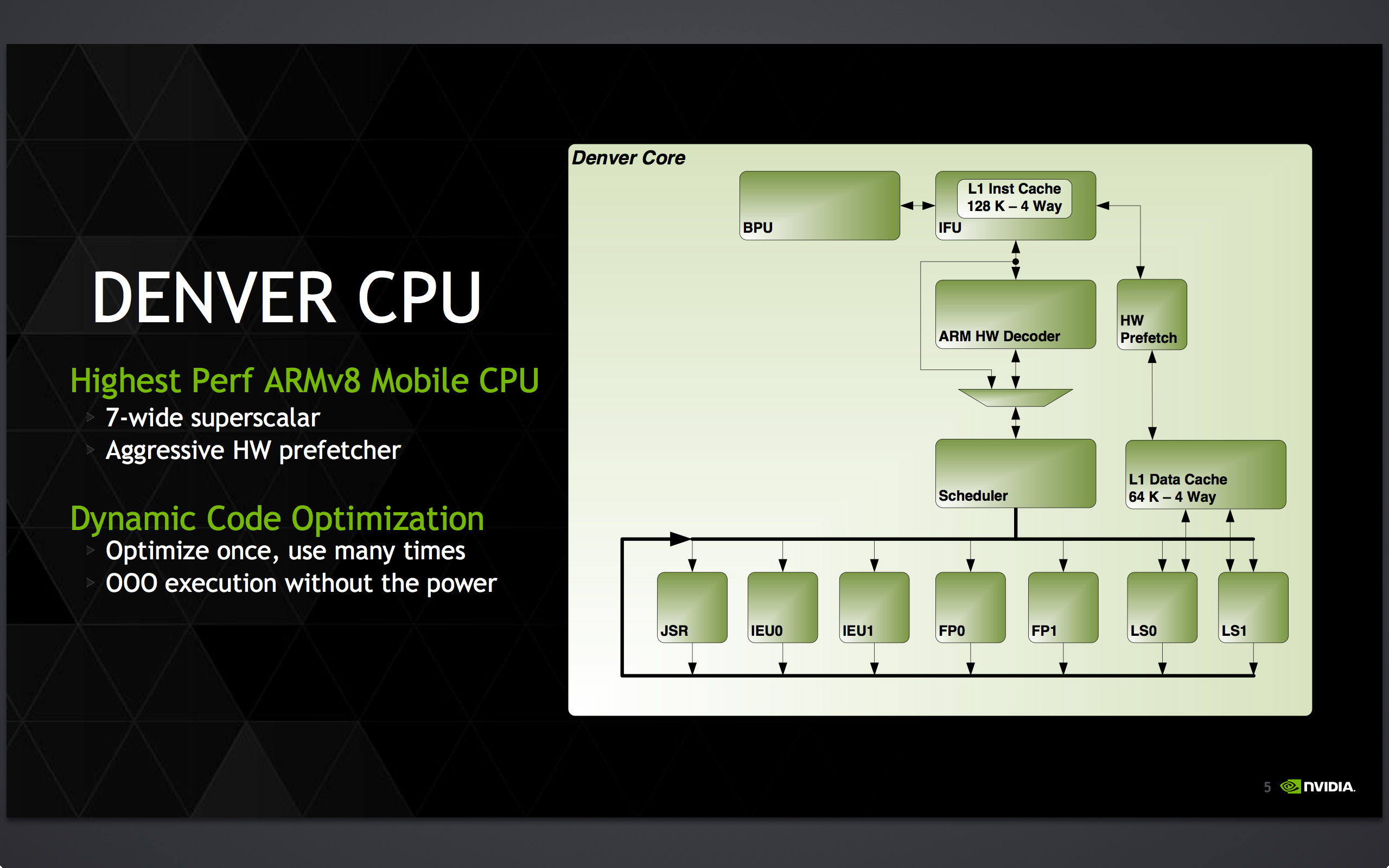
Denver’s Deep Details
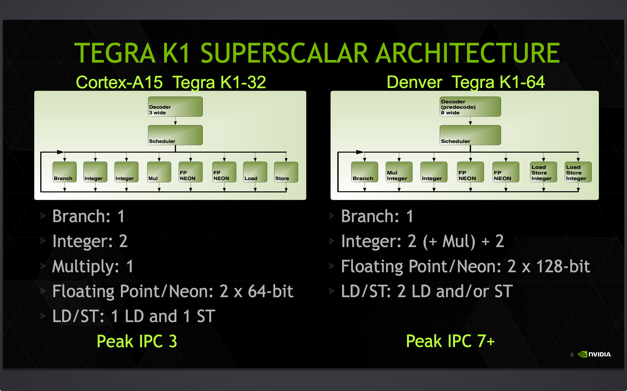
Due to NVIDIA’s choice not to pursue OoOE on Denver and simultaneously pursue a large, high performance core, Denver is by consumer standards a very wide CPU. With no OoOE hardware NVIDIA has been able to fill out Denver with execution units, with 7 slots’ worth of execution units backed by a native decoder wide enough to feed all of those units at once. The native decoder in particular is quite notable here, as most other CPU designs have narrower decoders that put a lower limit on their theoretical IPC. The Cortex-A15 cores in Tegra K1-32 for example only feature 3-wide decoders, despite having many more slots’ worth of execution units. Consequently a large decoder not only opens up the ability to increase IPC, but it is a sign that the CPU developer believes that their design is capable of keeping that many execution units busy enough to justify the cost of the wider decoder.
| NVIDIA CPU Core Comparison | ||||||
| K1-32 | K1-64 | |||||
| CPU | Cortex-A15 | NVIDIA Denver | ||||
| ARM ISA | ARMv7 (32-bit) | ARMv8 (32/64-bit) | ||||
| Issue Width | 3 micro-ops | 2 (ARM) or 7 (Native) micro-ops | ||||
| Pipeline Length | 18 stages | 15 stages | ||||
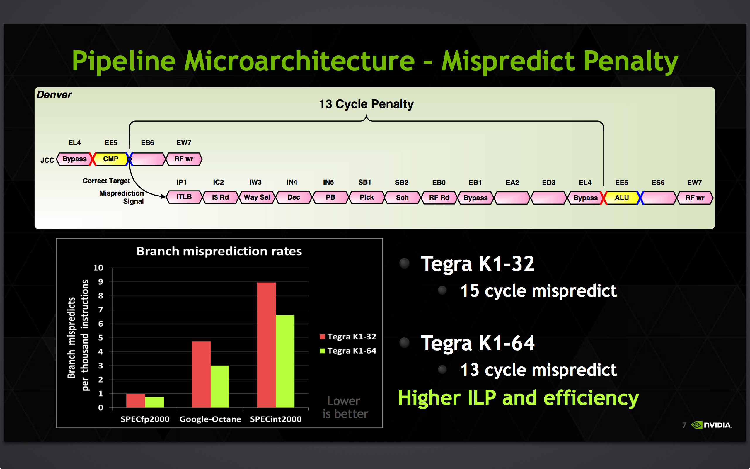
| Branch Mispredict Penalty | 15 cycles | 13 cycles | ||||
| Integer ALUs | 2 | 4 | ||||
| Load/Store Units | 1 + 1 (Dedicated L/S) | 2 (Shared L/S) | ||||
| Branch Units | 1 | 1 | ||||
| FP/NEON ALUs | 2x64-bit | 2x128-bit | ||||
| L1 Cache | 32KB I$ + 32KB D$ | 128KB I$ + 64KB D$ | ||||
| L2 Cache | 2MB | 2MB | ||||
These execution units themselves are fairly unremarkable, but none the less are very much at the heart of Denver. Compared again to Terga 4, there are twice as many load/store units, and the NEON units have been extended from 64-bits wide to 128-bits wide, allowing them to retire up to twice as much work per cycle if they can be completely filled.
Internally Denver executes instructions using the Very Long Instruction Word (VLIW) format, which is an instruction format that these days is more common with GPUs than it is CPUs, making it another vaguely GPU-like aspect of Denver. In VLIW all instructions are packed into a single word and sent through the pipeline at once, rather than handing each slot its own instruction. Each VLIW instruction is variable in length, and in turn the length of the operation is similarly variable, depending in part on factors such as the number of registers any given instruction operates upon. With a maximum VLIW instruction size of 32 bytes, this means that the number of operations a single instruction can contain is dependent on the operations, and it’s possible for large operations to fill out the VLIW early.
Another one of Denver’s unusual aspects is its internal instruction format, which is very different from ARMv7 or ARMv8. Though the specific format is beyond the scope of this article, it has long been rumored that Denver was originally meant to be an x86 design, with Denver’s underlying design and binary translation pairing intended to allow for an x86 implementation without infringing on any x86 hardware patents. Whether that is true or not, the end result of Denver is that owing to NVIDIA’s decision to solve their needs in software, NVIDIA was able to create an architecture whose design is decoupled from the actual instruction set it is executing.
Yet in spite of this architectural choice, Denver still needs to be able to execute ARM code as well as native code from binary translation, which leads to one more interesting wrinkle to Denver’s design. Denver has not one but two decoders, the native decoder and a proper ARM decoder. Designed to work in situations where Denver’s software optimizer is not worth running or can’t translate in time – such as with brand new code segments – the ARM decoder allows for Denver to directly decode ARM instructions.
The ARM decoder is not quite a backup, but it is not intended to be the main source of operations for Denver over the long run. Rather the bulk of the work for Denver should come from its binary translator, and only a small fraction of infrequently used code should hit the ARM decoder. At only 2 instructions wide this decoder is narrower than even A15’s decoder, not to mention it forms an entirely in-order pipeline that misses out on the instruction rescheduling and other optimizing benefits of the software code optimizer. Never the less it serves an important role in situations where Denver can’t use native code by giving it a means to immediately begin executing ARM code. This as a result makes Denver a kind of hybrid design, capable of executing either ARM instructions or NVIDIA’s own internal microcode.
Meanwhile Denver’s overall pipeline stands at 15 stages deep. Despite the overall width of Denver this actually makes the pipeline shorter than the 18 stage A15 by a few stages. And similarly, the penalty for branch mispredictions is down from 15 cycles in A15 to 13 cycles in Denver.
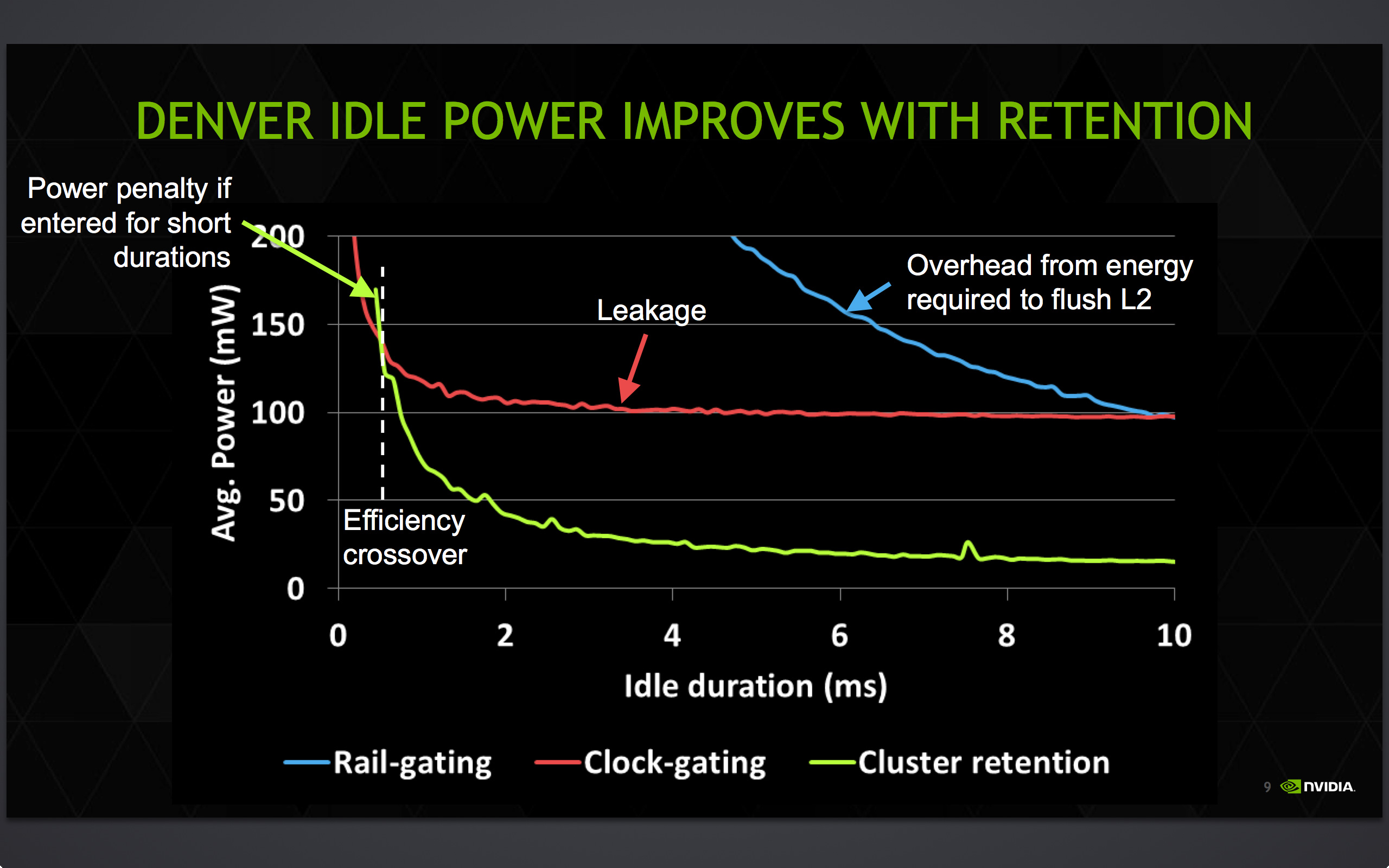
Last but not least, on the logical level NVIDIA has also been working to further reduce their power consumption through a new mode called CC4. CC4 is essentially a deeper state of sleep that’s not quite power-gating the entire CPU, but none the less results in most of the CPU being shut off. What ends up being retained in CC4 is the cache and what NVIDIA dubs the “architectural state” of the processor, a minimal set of hardware that allows the core voltage to drop below traditional Vmin and instead hold at just enough voltage to retain the contents of the cache and state, as no work needs to be done in this state. It's worth noting that we've seen similar power collapse states as far back as the A15 though, so the idea isn't necessarily new.
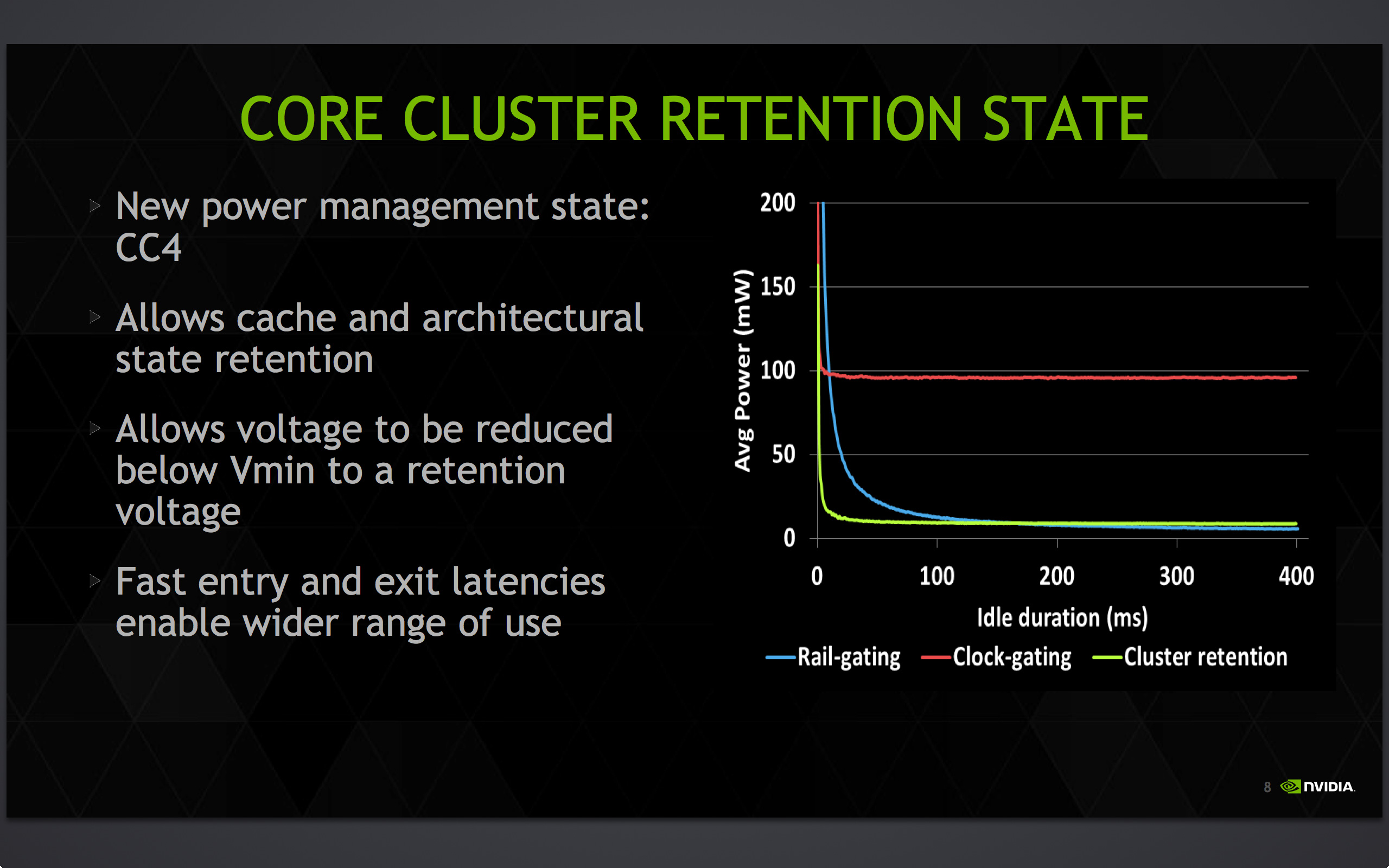
CC4 as a result is intended to be a relatively fast sleep state given its depth, with Denver able to enter and exit it faster than power-gating, and consequently it can be used more frequently. That said since it is deeper than other sleep states it is also slower than them, meaning the CPUIdle governor needs to take this into account and only select CC4 when there’s enough time to take advantage of it. Otherwise if Denver enters CC4 and has to come out of it too soon, the processor can end up wasting more power setting up CC4 than a very short CC4 duration would save.
Of course CC4 is just one of many factors in Denver’s power consumption. Hardware and software alike plays a role, from the silicon itself and the leakage characteristics of the physical transistors to the binary translation layer necessary for Denver to operate at its peak. And that brings us to the final and more crucial piece of the Denver puzzle: the binary translation layer.


169 Comments
View All Comments
melgross - Wednesday, February 4, 2015 - link
So, people only buy devices during the first three months?Impulses - Wednesday, February 4, 2015 - link
Apparently... Although getting the review in before February would've shut all these people up, cheapest place to get the Nexus 9 all thru the holidays was Amazon ($350 for 16GB) and they gave you until January 31 to return it regardless of when you bought it.Only reason I'm so keenly aware is I bought one as a February birthday gift, opened it last weekend just to check it was fine before the return window closed... Not much backlight bleed at all even tho it was manufacturerd in October (bought in late December), some back flex but it's going in a case anyway.
blzd - Friday, February 6, 2015 - link
What does the month of manufacture have to do with the back light bleed? You don't actually believe those "revision" rumors, do you?If you do, consider how practical it is for a hardware revision to come out 1 month after release. Then consider how one set of pictures on a Reddit post proves anything other than that their RMA worked as intended.
ToTTenTranz - Wednesday, February 4, 2015 - link
I wish more smartphone/tablet makers put as much thought into their external speakers as HTC does.Once having a HTC One M7, I simply can't go back to mono speakers at the back of devices.
Dribble - Wednesday, February 4, 2015 - link
Glad the review is here at last, next one a little bit quicker please :)UpSpin - Wednesday, February 4, 2015 - link
I have following issues with your review:1. You run webbrowser tests and derive CPU performance from it. That's nonsense! It's a web-browser test, and it won't be a CPU test whatever you do. If you want to test raw CPU performance you have to run native CPU test applications.
2. Your battery life analysis is based on false assumptions and you derive doubtful claims from it.
The error is quite evident on the iPad Air test. In your newly introduced white display test, with airplane on, CPU/GPU idling, etc. the iPad Air 2 has a battery life of 10:18 hours. Now in your web-browsing battery test with WiFi on and the CPU busy, the iPad Air 2 has a battery life of 9:76 hours. That's a difference of 4%. The Nexus 9 has a difference of 30%, the Note 4 15%, the Shield Tablet 25%.
You conclude: The Tegra K1 is inefficient. But I could also conclude that the A8 is inefficient and the Tegra K1 very efficient. The Tegra K1 needs significantly less power while idling, compared to the A8, which consumes always the same, mostly independent on the load. So finally, the A8 lacks any kind of power saving mode.
That's abstruse, but the consequence of your test. Or maybe your test is flawed from the beginning on.
3. " I suspect we’re looking at the direct result of the large battery, combined with an efficient display as the Nexus 9 can last as long as 15 hours in this test compared to the iPad Air 2’s 10 hours."
Sorry, but I don't get this either. The Nexus 9 has a 25.46 WHr battery, the iPad Air 2 a 27.3 WHr battery (+7%). The Nexus 9 has a 8.9" Display, the iPad Air 2 a 9.7". (+19% area). The resolution is the same, thus the DPI on the Nexus 9 higher. The display techonoly is the same, as you said in your analysis. So the difference must be related to something else, like a highly efficient idle SoC in the Nexus 9.
Andrei Frumusanu - Wednesday, February 4, 2015 - link
The battery life tests analysis is based on true facts on the technical workings of the SoC and its idle power states and we are confident in the resulting conclusions.JarredWalton - Wednesday, February 4, 2015 - link
Going along with what Andrei said, an SoC isn't "efficient" if it's doing no work -- the A8 may not have idle power as low as the K1-64, but when you're actually doing anything more with the tablet in question is when efficiency matters. It's clear that the Air 2 wins out over the Nexus 9 in some of those tests (GFX in particular). Doing more (or equivalent) work while using less power is efficient.Imagine this as an example of why idle power only matters so far: if you were to start comparing cars on how long they could idle instead of actual gas mileage, would anyone care? "Car XYZ can run for 20 hours off a tank while idle while Car ZYX only lasts 15 hours!" Except, neither car is actually doing what a car is suppose to do, which is take you from point A to point B.
The white screen test is merely a way to look at the idle power draw for a device, and by that we can get an idea of how much additional power is needed when the device is actually in use. Also note that it's possible due to the difference in OS that Android simply better disables certain services in the test scenario and iOS might be wasting power -- the fact that the battery life hardly changes in our Internet WiFi test even suggests that's the case.
To that end, the battery life of the N9 is still quite good. Get rid of the smartphones in the charts and it's actually pretty much class leading. But it's still odd that the NVIDIA SHIELD Tablet and iPad Air 2 only show a small drop between idle and Internet, while N9 loses 33% of its battery life.
ABR - Thursday, February 5, 2015 - link
Idle power is pretty important for real world use for tablets, for example where you are reading something and the system is just sitting there. Those "load web page then pause for xx time" test would probably be really good for measuring.JarredWalton - Thursday, February 5, 2015 - link
That's exactly what our Internet test does, which is why the 33% drop in battery life is so alarming. What exactly is going on that N9 loading a generally not too complex web page every 15 seconds or so kills battery life?