The iPhone 6 Review
by Joshua Ho, Brandon Chester, Chris Heinonen & Ryan Smith on September 30, 2014 8:01 AM EST- Posted in
- Smartphones
- Apple
- Mobile
- iPhone 6
A8: Apple’s First 20nm SoC
As has been customary for every iPhone launch since the company began publicly naming their SoCs, Apple has once again rolled out a new SoC for their latest line of phones. With the launch of the iPhone 6 series Apple is now up to their eight generation SoC, the appropriately named A8.
After a period of rapid change with the A6 and A7 SoCs – which introduced Apple’s first custom CPU design (Swift) and the first ARMv8 AArch64 design (Cyclone) respectively – A8 is a more structured and straightforward evolution of Apple’s SoC designs. Which is not to say that Apple hasn’t been busy tweaking their designs to extract ever-improved performance and power efficiency, as we’ll see, but our examination of A8 has not uncovered the same kind of radical changes that defined A6 and A7.
The heart and soul of A8 is as always the CPU and GPU. We’ll be taking a look at each of these individually in a moment, but from a high level both of these are evolutions of their predecessors found in A7. Apple’s GPU of choice remains Imagination’s PowerVR, having upgraded from the Series6 based G6430 to Imagination’s newer GX6450 design. Meanwhile Apple continues to develop their own CPUs and A8 packs their latest design, which is an enhanced version of the Cyclone core first introduced in A7.
Stepping away from the GPU and CPU for the moment, the biggest change about A8 is that it’s smaller. As discovered by Chipworks, A8 is being fabricated on TSMC’s new 20nm process, making the iPhone 6 among the first smartphones to be shipped with a 20nm SoC.
This move to 20nm is not unexpected, but nonetheless it is considerable for a couple of reasons. The first is that this means Apple has moved production over to TSMC’s 20nm HKMG Planar process, making this the first time an Apple SoC has been manufactured anywhere but a Samsung fab. There are numerous possible reasons for this – and not every reason needs to be technical – but from a process development standpoint it’s important to note that over the last few generations TSMC has been the leader among contract foundries, being the first to get new processes up and running for volume production.
| Apple A8 vs A7 SoCs | ||||
| Apple A8 (2014) | Apple A7 (2013) | |||
| Manufacturing Process | TSMC 20nm HKMG | Samsung 28nm HKMG | ||
| Die Size | 89mm2 | 102mm2 | ||
| Transistor Count | ~2B | "Over 1B" | ||
| CPU | 2 x Apple Enhanced Cyclone ARMv8 64-bit cores |
2 x Apple Cyclone ARMv8 64-bit cores |
||
| GPU | IMG PowerVR GX6450 | IMG PowerVR G6430 | ||
This move is also quite considerable because it means for the first time Apple is manufacturing their SoCs on a bleeding edge manufacturing process. Prior to this Apple has been slow to utilize new manufacturing processes, only finally utilizing a 28nm process in late 2013 for A7 over a year after 28nm first became available. The fact that we are seeing a 20nm SoC from Apple at a time when almost everyone else is still on 28nm indicates just how much the market has shifted over the last few years, and how Apple’s SoC development is now synchronized with the very edge of semiconductor fabrication technology.
Finally, the switch to 20nm is interesting because after the last couple of generations being so-called “half node” jumps – 45nm to 40nm to 32nm to 28nm – the jump from 28nm to 20nm is a full node jump (note that Apple didn't ever use 40nm, however). This means we are seeing a larger increase in transistor density than in the previous generations, and ideally a larger decrease in power consumption as well.
In practice TSMC’s 20nm process is going to be a mixed bag; it can offer 30% higher speeds, 1.9x the density, or 25% less power consumption than their 28nm process, but not all three at once. In particular power consumption and speeds will be directly opposed, so any use of higher clock speeds will eat into power consumption improvements. This of course gets murkier once we’re comparing TSMC to Samsung, but the principle of clock speed/power tradeoffs remains the same regardless.
Not accounting for minor differences between TSMC and Samsung, in an ideal case Apple is looking at 51% area scaling (the same design on 20nm can be no smaller than 51% of the die area at 28nm). In reality, nothing ever scales perfectly so the density gains will depend on the kind of I/C being laid down (logic, SRAM, etc.). For the complete chip a 60-70% scaling factor is going to be a better approximation, which for Apple means they’ve picked up a lot room to spend on new functionality and reducing their overall die size.
| Apple SoC Evolution | |||||
| CPU Perf | GPU Perf | Die Size | Transistors | Process | |
| A5 | ~13x | ~20x | 122m2 | <1B | 45nm |
| A6 | ~26x | ~34x | 97mm2 | <1B | 32nm |
| A7 | 40x | 56x | 102mm2 | >1B | 28nm |
| A8 | 50x | 84x | 89mm2 | ~2B | 20nm |
Meanwhile once again this year Apple opened up on die size and transistor counts. A8 weighs in at around 2 billion transistors, as opposed to the “over 1 billion” transistors found on A7. We also have the die size for A8 – 89mm2 – which is some 13% smaller than A7’s 102mm2 die. This makes it clear that Apple has chosen to split their transistor density improvements between adding features/performance and reducing their size, rather than going all-in on either direction.
In the case of using a bleeding edge node this is generally a good call, as Apple and TSMC will need to deal with the fact that chip yields at 20nm will not be as good as they are on the highly mature 28nm process. With lower chip yields, a smaller die will offset some of those yield losses by reducing the number of manufacturing flaws any given die touches, improving the overall yield.
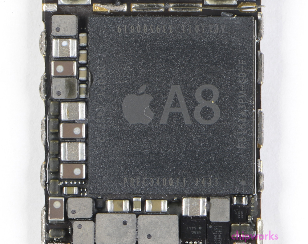
A8 With POP RAM Removed
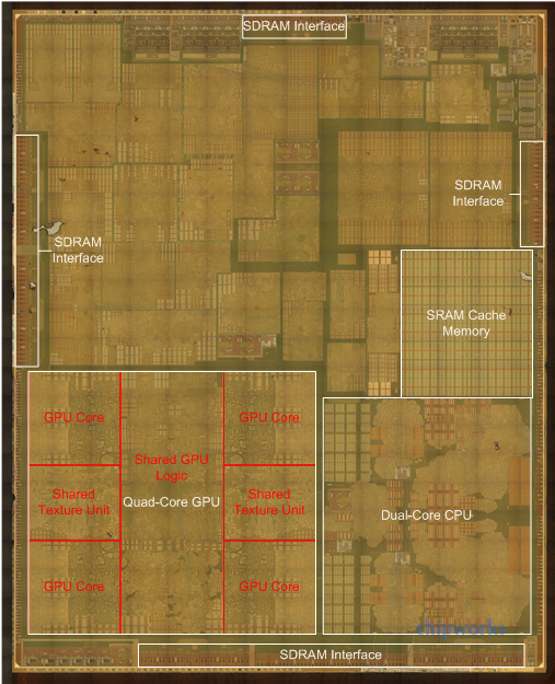
Moving on, looking at A8 we can see that Apple’s memory subsystem design has not significantly changed from A7. Once again Apple has placed an SRAM cache on the chip to service both the CPU and the GPU. Based on an examination of the die and of latency numbers, this L3 SRAM cache remains unchanged from A7 at 4MB. Meanwhile we also find a series of SDRAM interfaces which drive the A8’s package-on-package (POP) based main memory. Based on teardowns from iFixit, Apple is using 1GB of LPDDR3-1600, the same speed grade of LPDDR3 and capacity that they used for the iPhone 5s. iFixit has found both Hynix and Elpida memory in their phones, so Apple is once again using multiple sources for their RAM.
When we start poking at memory bandwidth we find that memory bandwidths are consistently higher than on A7, but only ever so slightly. This points to Apple having worked out further optimizations to make better use of the memory bandwidth they have available, since as we’ve previously determined they’re still using LPDDR3-1600 speeds.
| Geekbench 3 Memory Bandwidth Comparison (1 thread) | ||||||
| Stream Copy | Stream Scale | Stream Add | Stream Triad | |||
| Apple A8 1.4GHz | 9.08 GB/s | 5.37 GB/s | 5.76 GB/s | 5.78 GB/s | ||
| Apple A7 1.3GHz | 8.34 GB/s | 5.21 GB/s | 5.67 GB/s | 5.69 GB/s | ||
| A8 Advantage | 9% | 3% | 2% | 2% | ||
The Stream Copy score ends up being the biggest gain at 9%. Otherwise the rest of the benchmarks only show 2-3% memory bandwidth increases.
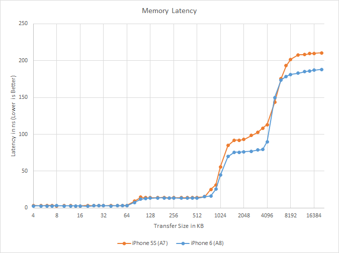
More interesting is memory latency, which shows some unexpected improvements once we get out of the L1 and L2 caches. At both the 1MB – 4MB region of the SRAM and 6MB+ region of main memory, memory latency is consistently lower on A8 versus A7. In both cases we’re looking at latencies about 20ns faster than A7. This identical 20ns gain tells us that that Apple is still doing main memory lookups after the L3 lookup fails, and this in turn means the 20ns gain we’re seeing is due to L3 cache optimizations. We have a couple of ideas for how Apple could have improved L3 latency by nearly 20% like this, but at this time with Apple staying quiet on their architecture like usual, it’s not apparent which of these ideas are the correct ones.
Turning our eyes back to A8 one final time, we find that while a lot of die space is occupied by the CPU, GPU, and SRAM (as we’d expect), there is also quite a bit of space occupied by other blocks Apple has integrated into their design. Without already knowing what you’re looking for these blocks are difficult to identify, but even without being able to do this we have a reasonable idea of what blocks Apple has integrated. Among these we’ll find audio controllers, USB controllers, video encoders/decoders, flash memory controllers, the camera ISP, and of course all kinds of interconnect.
All of these blocks are fixed function hardware (or at best, limited flexibility DSPs), which are equally important to not only the A8’s functionality but power efficiency. By assigning tasks to dedicated hardware Apple does spend some die space on that hardware, but in return these blocks are more efficient than doing those tasks entirely in software. Hence Apple (and SoC designers in general) have a strong incentive to offload as much work as possible to keep power consumption in check. This move towards more fixed function hardware is part of a general “wheel of reincarnation” cycle that has been a constant in processor design over the years, which sees a continuous shift between fixed function and programmable hardware. SoCs, for the most part, are still going towards fixed function hardware, and this should continue for a while yet.

In any case, while we can’t identify individual blocks on A8 we do know that Apple has added a few features to A8 that are present in some form or another among these blocks. New to A8 is some mix of H.265 (HEVC) hardware, which would be necessary to enable the FaceTime over H.265 functionality that is being introduced on the iPhone 6. Apple’s “desktop class scaler” that is used for handling non-native resolution applications and for down-sampling the internal rendering resolution of the iPhone 6 Plus would also be present here.


531 Comments
View All Comments
elajt_1 - Friday, October 3, 2014 - link
(@melgross) And to call you one would be an insult to an idiot.Apart from the rage, I think it was he made some valid points.
Jimrod - Tuesday, September 30, 2014 - link
You mad bro?rational_wannabe - Tuesday, September 30, 2014 - link
You have serious issues. So it's OK for Samsung to sell their plastic crap for the same amount of money? Nice way of rationalizing things...danbob999 - Tuesday, September 30, 2014 - link
Yeah it's OK since there is nothing wrong with plastic. It absorbs shock, is light and do not block wireless signal. Perfect material for a phone. It is also durable enough. How many people replace their phone because the plastic is cracked? Not much. People replace their phone either because the screen is broken, it was damaged by liquid or simply because it is too slow/old.Apple has been selling phones which are cheaper to produce for years at the same price (or higher) than the competition. Smaller phones tend to be cheaper, because the display is cheaper, the battery is cheaper, and the rest cost the same. So even by using plastic, Samsung phones cost more to produce so I fail to see how they can be labeled as "cheap".
blackcrayon - Tuesday, September 30, 2014 - link
Apple is spending far more in developing the phone in other areas though. Writing the OS, designing custom SoCs, etc.danbob999 - Tuesday, September 30, 2014 - link
Designing custom SoCs is an investment. It isn't supposed to raise the cost of the phone.Samsung also design some of its own SoCs and even manufacture them.
The OS is debatable. But from a hardware perspective Samsung phones (at least the high end ones) are definitely not cheap, even if they use plastic.
Parhel - Tuesday, September 30, 2014 - link
R&D should affect the cost of the product? That's not how it works . . .Parhel - Tuesday, September 30, 2014 - link
Ugh.. meant to say R&D "shouldn't". To state it plainly, R&D may be an investment, but it's still an expense. The cost needs to be recouped, and they make money by selling phones, so . . . you do the math.danbob999 - Tuesday, September 30, 2014 - link
Of course they have to make money. But spending more in software development, R&D or marketing doesn't make their phone any less "cheap". I was replying to someone saying that Samsung phones were "cheap" because they were in plastic. The fact is that Samsung phones tend to be more expensive than iPhones to make, because the cost of the components is higher, despite any savings made by using a plastic shell.akdj - Friday, October 3, 2014 - link
Only BECAUSE it takes my Note3 twice the cores, at twice the clock speed with three times the amount RAM to FINALLY close the gap on performance. Almost. My 5s is still quicker playing Asphalt8, manipulating photos, even rendering VIDEO! Most likely the latter because of the extreme lack of interet in the development community (other than game ports) to 'build out' apps and software. And that sucks! I love my Note 3--- coming from the original its a massive upgrade. That said, Samsung is using stock, off the shelf SoCs ....indeed 'produced' by them as they've got the capabilities to cook bake and roll out silicon BUT they've chosen to increase horsepower, drop the gearing ratios and add a stage III nirrous kit 'built' and low level programmed with basic ARM instructions and a radical slather of Peanut Butter JavaScript to wade through just for TouchWiz. By the time you open an app, you're at 85-90% RAM usage. I've got a N3. I like it and I'm not getting rid of it. It serves it's purpose for our business perfectly. But AS a business owner and one that relies on creative talent to make it 'work' I find your comment very VERY ill informed and 'ignorant' ...no to be a dick. But yes, R&D is definitely a percentage figured into the equation with BOM. As well, the software development, A8 & the second generation 64bit processor with a faster GPU, more efficient memory managment with the SoC 4mb buffer and iOS 8 itself are expenses. Paid to a LOT of talent! For crying out loud, they developed a new CODE! And a spectacular one at that! Free lessons are everywhere and if you're experienced, have a macbook laying around, download the latest XCode and you'll have Swift down in a weekend. Not to mentioned the low level 'Metal' instruction set to eliminate the OpGL ES overhead ...allowing developers 'direct' (hence, 'Metal') access to the GPU ...if you're at all curious on how incredible this development most consumers will NEVER know about ...check out Unreal 4's site, the UR4 engine and what they've done with Metal. You can download their patio presentation frim WWDC in the app store. It's absolutley amazing. Samsung's phones are spendy because they're licensing Wacom, using active digitizers few are able use (until this evolution, three's a charm I guess), massive batteries, a horrid looking bezel that's rigid for sure, but then again, this is the first I've seen people, on purposes bending phones, and that's not a real life issue or even concern. I shared earlier, somehow my nine year old son has managed to keep his iPod touch fifth gen in perfect non bent and scratch free condition. Two years. Lotsa boogers and bumps but no dents, no dings, scratches or 'display marks' without screen protection. Guesses can be made in physical pieces. Even how long (labor pricing) to produce a single unit. But development of actual silicon, low level optimization to your non fragmented operating system, 64bit technology 24 months ahead of the industry and obvious benefits from the 20nm A8. iOS 8 (and its counterpart more than ever, OS X 10.10) and its ability to aggregate our information across devices, handoff calls, emails, texts or whatever the hell you're doing on your iPad ....get distracted, fall out and when you turn your iMac or MBP on, there's the email you were working on. Ready for you to finish. The web page you were reading or the movie your were watching ...vice versa too. Start on your computer a doc, and open your iPhone, there'll be a small 'doc' icon signifying you're working on something and you're able to finish it here! Forget the phone downstairs, your in bed reading before sleep, phone rings...no worries. Answer it on your iPad. AirDrop between laptop, tablet and phone, MacPro and ipad....iPhone to your iMac, slick n quick.Of course, then there's the whole 'build quality' argument. Where designers, reviewers, and the public ALL Seem to agree. The iPhone SNOKES Samsung's BQ. Period. They're like jewelry, true and real 'art'. Each phone has been an engineering marvel. Samsung? Are you kidding me? Other than their goofy, curvy, earthy S3 baby blue tangent, their 'rectangle' phone lacks ANY design fundamentals much less achievements.
When you sell as MANY pieces as Apple does, costs come down. For the 'pieces'. But the machining process (2 year cycle) is entirely changed. Fusion welding and sapphire 'plants', robotics and laser/chamfered edging with incredible attention to detail are just a couple of the hundreds of THOUSANDS of re-tooling the facilities for the latest 'build'. And after a couple of hours today with the 6 & 6+ as we anxiously await ours, with an open mind (& as an ambidextrous user of Android and iOS Windows and OS X) --- NOTHING on the Internet does justice to the phone itself. It's. Absolutely. AMAZING!