The NVIDIA GeForce GTX 980 Review: Maxwell Mark 2
by Ryan Smith on September 18, 2014 10:30 PM ESTMeet the GeForce GTX 980
For the physical design of the reference GeForce GTX 980, NVIDIA is clearly iterating on previous designs rather than coming up with something from scratch. With that said however, the idiom of “if it ain’t broke, don’t fix it” has been very applicable to NVIDIA over the last year and a half since the launch of the GTX Titan and its high-end cooler. The GTX Titan’s cooler set a new bar in build quality and performance for a blower design that is to this day unmatched, and for that reason NVIDIA has reused this design for the GTX 780, GTX 780 Ti, GTX Titan Black, and now the GTX 980. What this means for the GTX 980 is that its design comes from a very high pedigree, one that we believe shall serve it well.
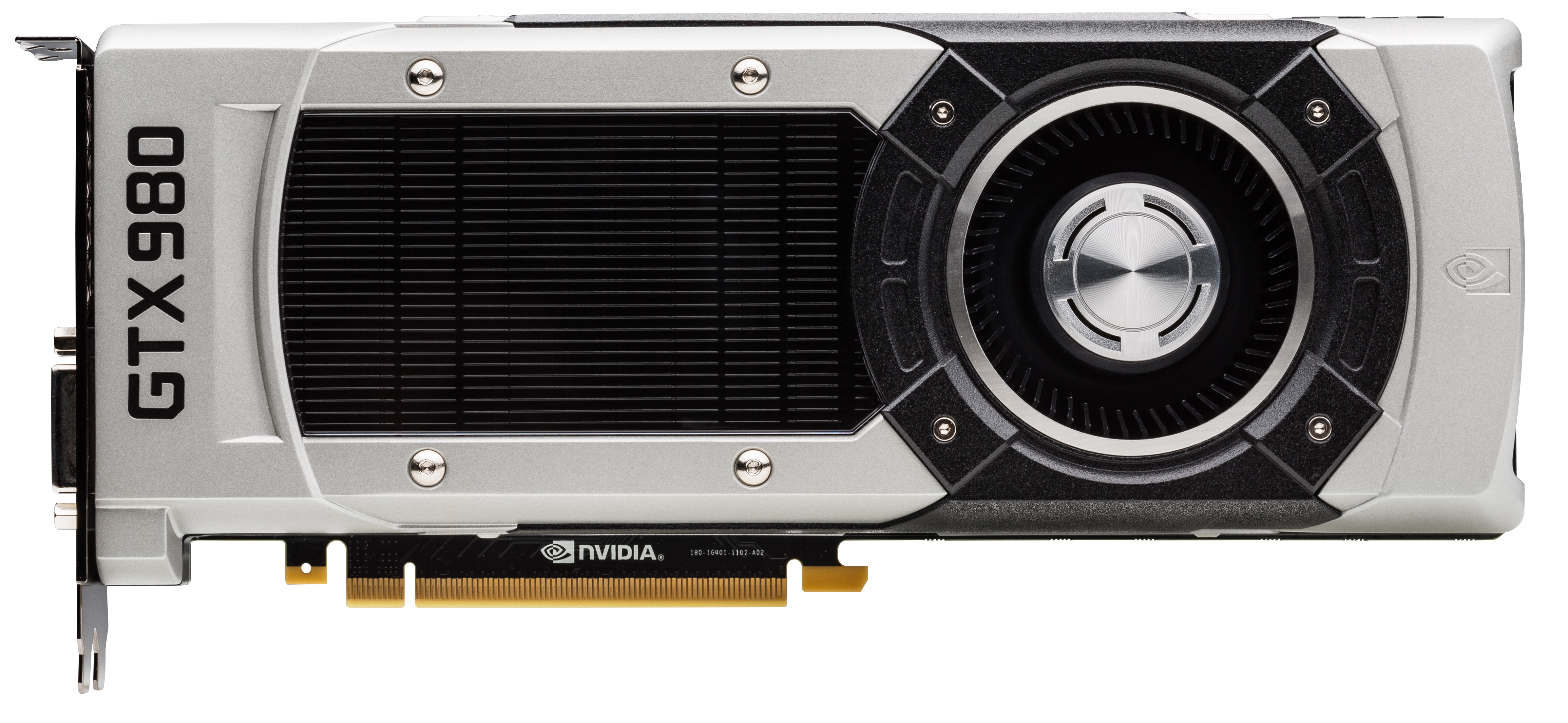
At a high level, GTX 980 recycles the basic cooler design and aesthetics of GTX 780 Ti and GTX Titan Black. This means we’re looking at a high performance blower design that is intended to offer the full heat-exhaustion benefits of a blower, but without the usual tradeoff in acoustics. The shroud of the card is composed of cast aluminum housing and held together using a combination of rivets and screws. NVIDIA has also kept the black accenting first introduced by its predecessors, giving the card distinct black lettering and a black tinted polycarbonate window. The card measures 10.5” long overall, which again is the same length as the past high-end GTX cards.
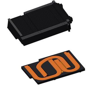
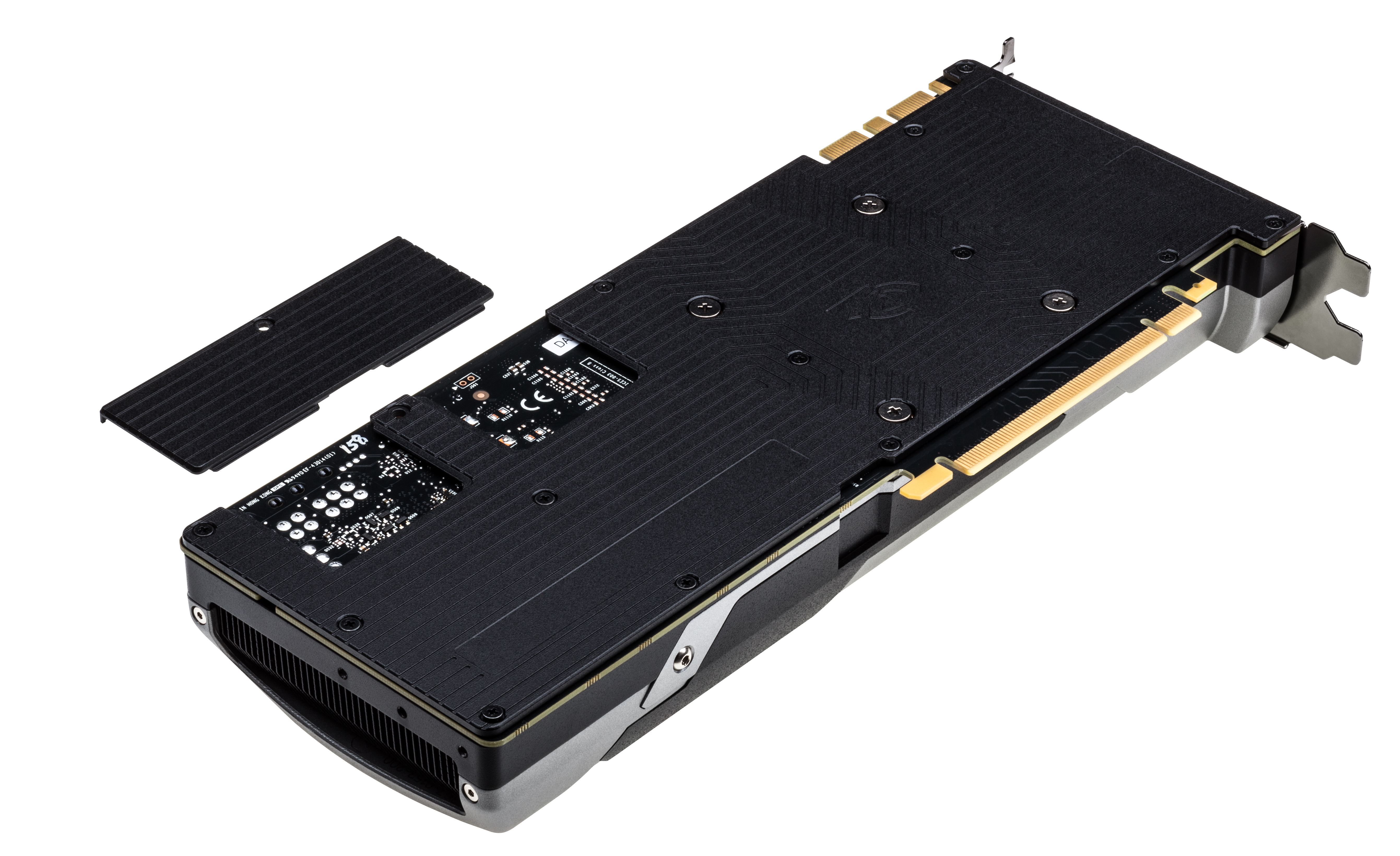
Cracking open the card and removing the shroud exposes the card’s fan and heatsink assembly. Once again NVIDIA is lining the entire card with an aluminum baseplate, which provides heatsinking capabilities for the VRMs and other discrete components below it, along with providing additional protection for the board. The primary GPU heatsink is fundamentally the same as before, retaining the same wedged shape and angled fins.
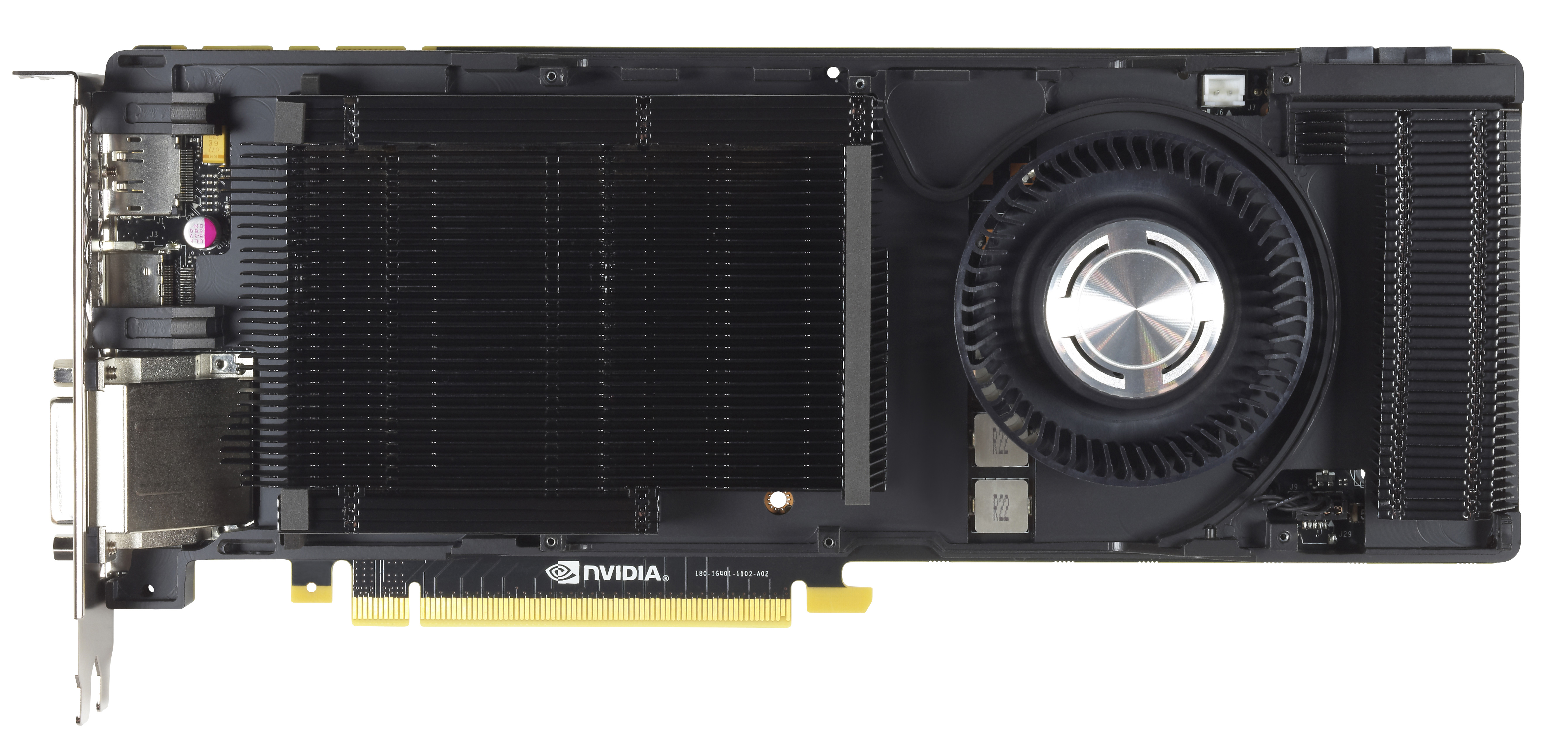
However in one of the only major deviations from the earlier GTX Titan cooler, at the base NVIDIA has dropped the vapor chamber design for a simpler (and admittedly less effective) heatpipe design that uses a trio of heatpipes to transfer heat from the GPU to the heatsink. In the case of the GTX Titan and other GK110 cards a vapor chamber was deemed necessary due to the GPU’s 250W TDP, but with GM204’s much lower 165W TDP, the advanced performance of the vapor chamber should not be necessary. We would of course like to see a vapor chamber here anyhow, but we admittedly can’t fault NVIDIA for going without it on such a low TDP part.
Drilling down to the PCB, we find a PCB design not all that far removed from NVIDIA’s GK110 PCBs. At the heart of the card is of course the new GM204 GPU, which although some 150mm2 smaller than GK110, is still a hefty GPU on its own. Paired with this GPU are the 8 4Gb 7GHz Samsung GDDR5 modules that surround it, composing the 4GB of VRAM and 256-bit memory bus that GM204 interfaces with.
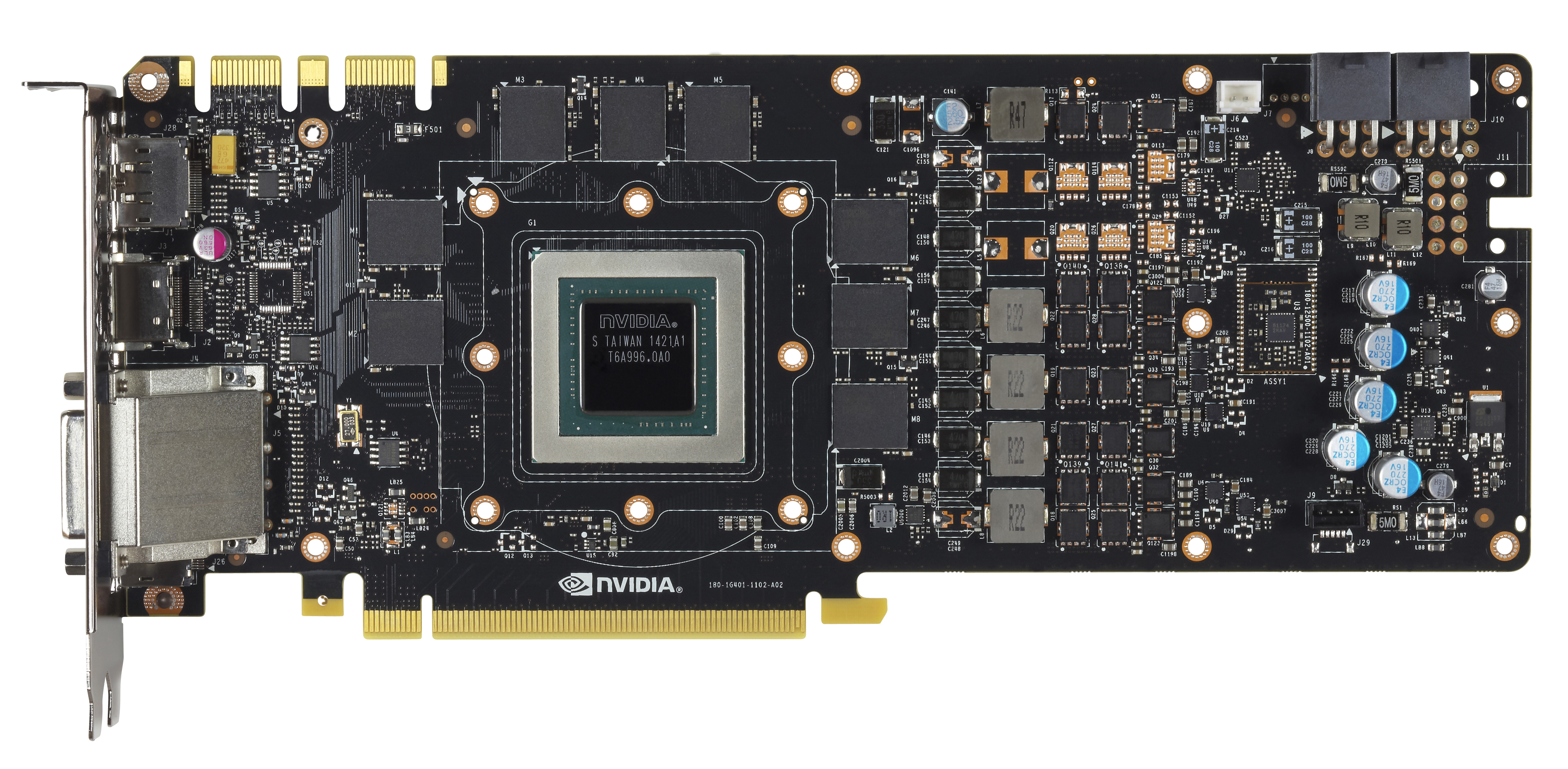
Towards the far side of the PCB we find the card’s power delivery components, which is composed of a 4+1 phase design. Here NVIDIA is using 4 power phases for the GPU itself, and then another phase for the GDDR5. Like the 5+1 phase design on GK110 cards, this configuration is more than enough for stock operations and mild overclocking, however hardcore overclockers will probably end up gravitating towards custom designs more with more heavily overbuilt power delivery systems. Though it is interesting to note that NVIDIA’s design has open pads for 2 more power phases, meaning there is some kind of headroom left in the PCB design. Meanwhile feeding the power delivery system is a pair of 6pin PCIe sockets, giving the card a combined power delivery ceiling of 225W, which is still well above the maximum TDP NVIDIA allows for this card.
What may be the most interesting – or at least most novel – aspect of GTX 980 isn’t even found on the front side of the card, but rather it’s what’s found on the back side. Back after a long absence is a backplate for the card, which runs the entire length of the card and completely covers the back side of the PCB, leaving no element exposed except for the SLI connectors above it and the PCIe connector below it.
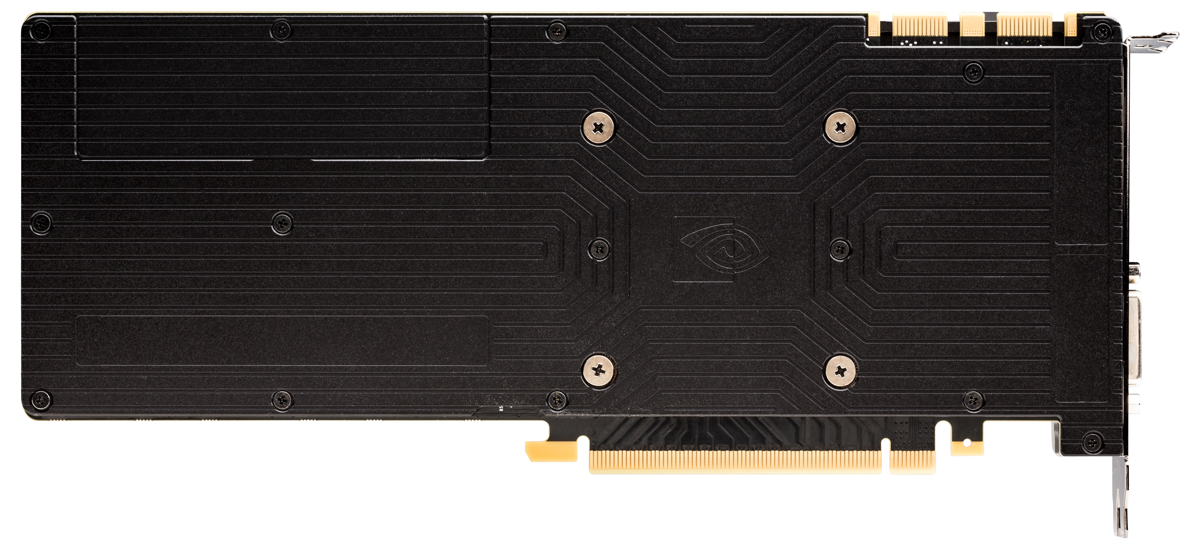
Generally speaking backplates are nice to have on video cards. Though they don’t provide any kind of meaningful mechanical/thermal benefit, they do serve to protect a card by reducing how much of the relatively vulnerable PCB is exposed, and similarly protect the user by keeping them from getting jabbed by the soldered tips of discrete components. However backplates typically come with one very big drawback, which is that the 2mm or so of space they occupy is not really their space, and encroaches on anything above it. For a single video card this is not a concern, but when pairing up video cards for SLI, if the cards are directly next to each other this extra 2mm makes all the difference in the world for cooling, blocking valuable space for airflow and otherwise suffocating the card unlucky enough to get blocked.
In more recent years motherboard manufacturers have done a better job of designing their boards by avoiding placing the best PCIe x16 slots next to each other, but there are still cases where these cards must be packed tightly together, such as in micro-ATX cases and when utilizing tri/quad-SLI. As a result of this clash between the benefits and drawbacks of the backplate, for GTX 980 NVIDIA has engineered a solution that allows them to include a backplate and simultaneously not impede the airflow of closely packed cards, and that is a partially removable backplate.
For GTX 980 a segment of the backplate towards the top back corner is detachable from the rest, and removing it exposes the PCB underneath. Based on studying the airflow of video cards with and without a backplate, NVIDIA tells us that they have been able to identify what portion of the backplate is responsible for impeding most of the airflow in an SLI configuration, and that they in turn have made this segment removable so as to be able to offer the full benefits of a backplate while also mitigating the airflow problems. Interestingly this segment is actually quite small – it’s only 34mm tall – making it much shorter than the radial fan on the front of the card, but NVIDIA tells us that this is all that needs to be removed to let a blocked card breathe. In our follow-up to the GTX 980 next week we will be looking at SLI performance, and this will include measuring the cooling impact of the removable backplate segment.
Moving on, beginning with GTX 980 NVIDIA’s standard I/O configuration has dramatically changed, and so for that matter has the design of their I/O shield. First introduced with GTX Titan Z and now present on GTX 980, NVIDIA has been working to maximize the amount of airflow available through their I/O bracket by replacing standard rectangular vents with triangular vents across the whole card. This results in pretty much every square centimeter of the card not occupied by an I/O port having venting through it, leading to very little of the card actually being blocked by the I/O shield.
Meanwhile starting with GTX 980, NVIDIA is introducing their new standard I/O configuration. NVIIDA has finally dropped the second DL-DVI port, and in its place they have installed a pair of full size DisplayPorts. This brings the total I/O configuration up to 1x DL-DVI-I, 3x DisplayPort 1.2, and 1x HDMI 2.0. The inclusion of more DisplayPorts has been a long time coming and I’m glad to see that NVIDIA has finally gone this route. DisplayPorts offer more functionality than any other type of port and can easily be converted to HDMI or SL-DVI as necessary. More importantly for NVIDIA, with 3 DisplayPorts NVIDIA can now drive 3 G-Sync monitors off of a single card, making G-Sync Surround viable for the first time.
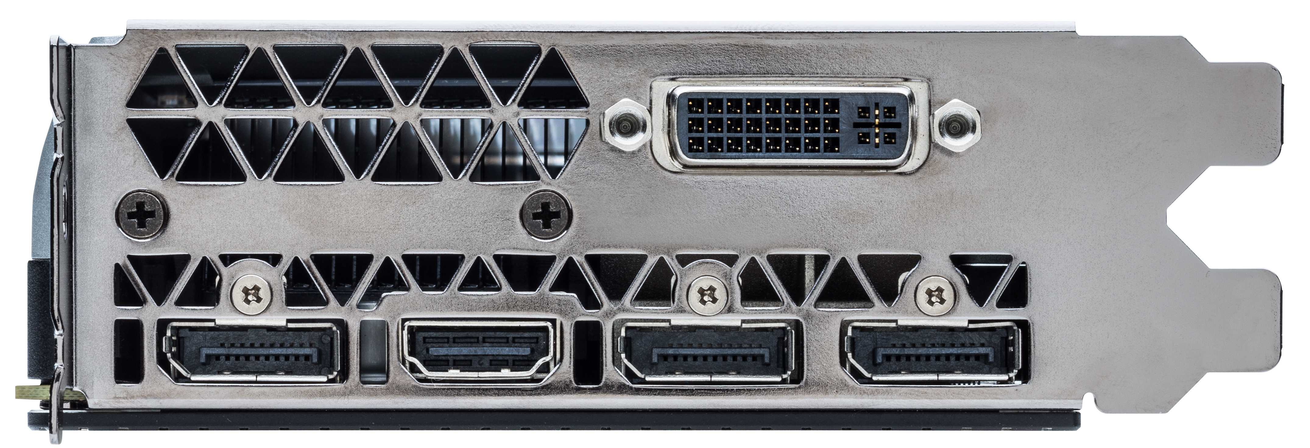
Speaking of I/O, we’ll briefly note that NVIDIA’s SLI connectors are still present, with the pair of connectors allowing up to quad-SLI. However we’d also note that this also means that for anyone hoping that NVIDIA would have an all-PCIe multi-GPU solution analogous to AMD’s XDMA engine, Maxwell 2 will not be such a product. Physical bridges are still necessary for SLI, with NVIDIA splitting up the workload over SLI and PCIe in the case of very high resolutions such as 4K.
Wrapping up our look at the physical build quality of the GTX 980, NVIDIA has done a good job iterating on what was already an excellent design with the GTX Titan and its cooler. The backplate, though not a remarkable difference, does give the card that last bit of elegance that GTX Titan and its GK110 siblings never had, as the card is now clad in metal from top to bottom. As silly as it sounds, other than the PCIe connector the GTX 980 may as well be a complete consumer electronic product of its own, as it’s certainly built like one.
Finally, along with the hardware we also want to quickly summarize the GPU Boost 2.0 limits NVIDIA has chosen for the GTX 980, to better illustrate what the card is capable of. Like the other high-end NVIDIA cards before it, NVIDIA has opted to set the GTX 980’s temperature target at 80C, with a maximum target of 91C and an absolute thermal threshold of 95C. Meanwhile the card’s 165W TDP limit can be increased by as much as 25% to 206W, or 41W over its reference limit.
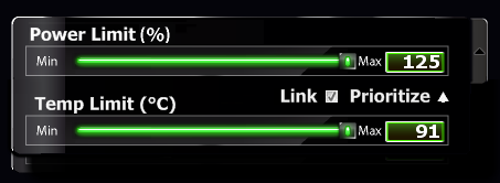
It’s interesting to note that despite the fact that the GTX Titan cooler was designed for a 250W card, GTX 980 will still see some temperature throttling under heavy, sustained loads. NVIDIA seems to have invested most of their cooling gains into acoustics, which has produced a card with amazing acoustic performance given the combination of the blower and the chart-topping performance, but it has also produced a card that is still going to throttle from time to time.


274 Comments
View All Comments
Frenetic Pony - Friday, September 19, 2014 - link
This is the most likely thing to happen, as the transition to 14nm takes place for intel over the next 6 months those 22nm fabs will sit empty. They could sell capacity at a similar process to TSMC's latest while keeping their advantage at the same time.nlasky - Friday, September 19, 2014 - link
Intel uses the same Fabs to produce 14nm as it does to produce 22nmlefty2 - Friday, September 19, 2014 - link
I can see Nvidia switching to Intel's 14nm, however Intel charges a lot more than TSMC for it's foundry services (because they want to maintain their high margins). That would mean it's only economical for the high end cardsSeanJ76 - Friday, September 19, 2014 - link
What a joke!!!! 980GTX doesn't even beat the previous year's 780ti??? LOL!! Think I'll hold on to my 770 SC ACX Sli that EVGA just sent me for free!!Margalus - Friday, September 19, 2014 - link
uhh, what review were you looking at? or are you dyslexic and mixed up the results between the two cards?eanazag - Friday, September 19, 2014 - link
Nvidia would get twice as many GPUs per wafer on a 14nm process than 28nm. Maxwell at 14nm would blow Intel integrated and AMD out of the water in performance and power usage.That simply isn't the reality. Samsung has better than 28nm processes also. This type of partnership would work well for Nvidia and AMD to partner with Samsung on their fabs. It makes more sense than Intel because Intel views Nvidia as a threat and competitor. There are reasons GPUs are still on 28nm and it is beyond process availability.
astroidea - Friday, September 19, 2014 - link
They'd actually get four times more since you have to considered the squared area. 14^2*4=28^2emn13 - Saturday, September 20, 2014 - link
Unfortunately, that's not how it works. A 14nm process isn't simply a 28nm process scaled by 0.5; different parts are scaled differently, and so the overall die area savings aren't that simple to compute.In a sense, the concept of a "14nm" process is almost a bit of a marketing term, since various components may still be much larger than 14nm. And of course, the same holds for TSMC's 28nm process... so a true comparison would require more knowledge that you or I have, I'm sure :-) - I'm not sure if intel even releases the precise technical details of how things are scaled in the first place.
bernstein - Friday, September 19, 2014 - link
no because intel is using their 22nm for haswell parts... the cpu transition ends in a year with the broadwell xeon-ep... at which point almost all the fabs will either be upgraded or upgrading to 14nm and the rest used to produce chipsets and other secondary die'snlasky - Saturday, September 20, 2014 - link
yes but they use the same fabs for both processes