The NVIDIA GeForce GTX 980 Review: Maxwell Mark 2
by Ryan Smith on September 18, 2014 10:30 PM ESTSynthetics
As always we’ll also take a quick look at synthetic performance. These tests mainly serve as a canary for finding important architectural changes, and with the exception of pixel throughput we are not expecting any major changes for GTX 980 and GM204.
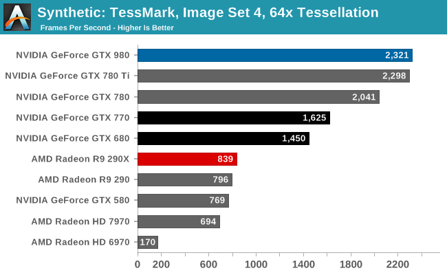
GM204 is designed to have an ever-so-slightly higher triangle throughput rate than GK110 – 16 tris/clock versus 15 tris/clock, and sure enough the GTX 980 comes out on top in TessMark, slightly edging out the GTX 780 Ti. The difference is only very slight here, and though GM204 should be a bit more powerful than GK110 in practice it’s a dead heat.
Moving on, we have our 3DMark Vantage texture and pixel fillrate tests, which present our cards with massive amounts of texturing and color blending work. These aren’t results we suggest comparing across different vendors, but they’re good for tracking improvements and changes within a single product family.
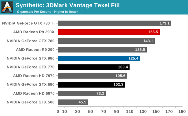
Beginning with Maxwell NVIDIA reduced their texture-to-compute ratio from 12:1 to 16:1. As a result of this change Maxwell GPUs have fewer texture units than comparable Kepler GPUs. Compounding this effect is the fact that Maxwell CUDA cores are more efficient than Kepler CUDA cores, leading to NVIDIA placing fewer cores overall and further reducing the texture fill rate.
As a result the GTX 980 is not texture fillrate competitive with any of the GK110 cards. It is competitive with the GK104 cards, but only because these cards had the same number of texture units at 128. NVIDIA has told us that they believe this new ratio is a better fit for modern workloads, and judging from the performance we’re seeing elsewhere it would appear that NVIDIA is right.
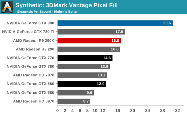
On the other hand, thanks to NVIDIA’s newer 3rd generation delta color compression technology, our 3DMark pixel fillrate performance is through the roof. GTX 980 comes very close to doubling the throughput of our GK110 cards and more than doubles the throughput of the GK104 cards, reflecting the fact that it has 64 ROPs and more importantly has the available bandwidth to put them to good use.
This benchmark in a nutshell is why NVIDIA can deliver chart-topping performance despite having only 2/3rds the memory bandwidth of GTX 780 Ti. By improving their color compression to this point, NVIDIA can significantly reduce their memory bandwidth requirements Maxwell 2, allowing them to do more with less. In real games the result won’t be anywhere near this remarkable since this is a pure pixel fillrate test, but it goes to show that NVIDIA has been able to expand their effective memory bandwidth in concert with their ROP and shader performance improvements.


274 Comments
View All Comments
jmunjr - Friday, September 19, 2014 - link
Wish you had done a GTX 970 review as well like many other sites since way more of us care about that card than the 980 since it is cheaper.Gonemad - Friday, September 19, 2014 - link
Apparently, if I want to run anything under the sun in 1080p cranked to full at 60fps, I will need to get me one GTX 980 and a suitable system to run with it, and forget mid-ranged priced cards.That should put an huge hole in my wallet.
Oh yes, the others can run stuff at 1080p, but you have to keep tweaking drivers, turning AA on, turning AA off, what a chore. And the milennar joke, yes it RUNS Crysis, at the resolution I'd like.
Didn't, by any chance, the card actually benefit of being fabricated at 28nm, by spreading its heat over a larger area? If the whole thing, hipothetically, just shrunk to 14nm, wouldn't all that 165W of power would be dissipated over a smaller area (1/4 area?), and this thing would hit the throttle and stay there?
Or by being made smaller, it would actually dissipate even less heat and still get faster?
Yojimbo - Friday, September 19, 2014 - link
I think that it depends on the process. If Dennard scaling were to be in effect, then it should dissipate proportionally less heat. But to my understanding, Dennard scaling has broken down somewhat in recent years, and so I think heat density could be a concern. However, I don't know if it would be accurate to say that the chip benefited from the 28nm process, since I think it was originally designed with the 20nm process in mind, and the problem with putting the chip on that process had to do with the cost and yields. So, presumably, the heat dissipation issues were already worked out for that process..?AnnonymousCoward - Friday, September 26, 2014 - link
The die size doesn't really matter for heat dissipation when the external heat sink is the same size; the thermal resistance from die to heat sink would be similar.danjw - Friday, September 19, 2014 - link
I would love to see these built on Intel's 14nm process or even the 22nm. I think both Nvidia and AMD aren't comfortable letting Intel look at their technology, despite NDAs and firewalls that would be a part of any such agreement.Anyway, thanks for the great review Ryan.
Yojimbo - Friday, September 19, 2014 - link
Well, if one goes by Jen-Hsun Huang's (Nvidia's CEO) comments of a year or two ago, Nvidia would have liked Intel to manufacture their SOCs for them, but it seems Intel was unwilling. I don't see why they would be willing to have them manufacture SOCs and not GPUs being that at that time they must have already had the plan to put their desktop GPU technology into their SOCs, unless the one year delay between the parts makes a difference.r13j13r13 - Friday, September 19, 2014 - link
hasta que no salga la serie 300 de AMD con soporte nativo para directx 12Arakageeta - Friday, September 19, 2014 - link
No interpretation of the compute graphs whatsoever? Could you at least report the output of CUDA's deviceQuery tool?texasti89 - Friday, September 19, 2014 - link
I'm truly impressed with this new line of GPUs. To be able to acheive this leap on efficiency using the same transistor feature size is a great incremental achievement. Bravo TSMC & Nvidia. I feel comfortable to think that we will soon get this amazing 980 performance level on game laptops once we scale technology to the 10nm process. Keep up the great work.stateofstatic - Friday, September 19, 2014 - link
Spoiler alert: Intel is building a new fab in Hillsboro, OR specifically for this purpose...