The NVIDIA GeForce GTX 980 Review: Maxwell Mark 2
by Ryan Smith on September 18, 2014 10:30 PM EST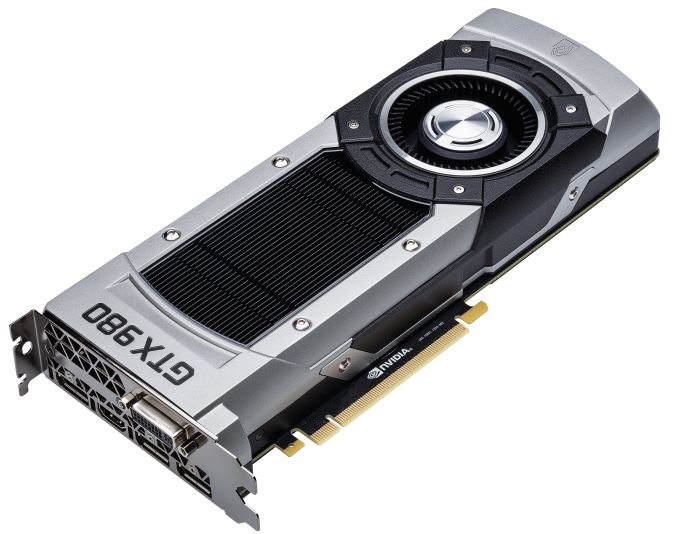
At the risk of sounding like a broken record, the biggest story in the GPU industry over the last year has been over what isn’t as opposed to what is. What isn’t happening is that after nearly 3 years of the leading edge manufacturing node for GPUs at TSMC being their 28nm process, it isn’t being replaced any time soon. As of this fall TSMC has 20nm up and running, but only for SoC-class devices such as Qualcomm Snapdragons and Apple’s A8. Consequently if you’re making something big and powerful like a GPU, all signs point to an unprecedented 4th year of 28nm being the leading node.
We start off with this tidbit because it’s important to understand the manufacturing situation in order to frame everything that follows. In years past TSMC would produce a new node every 2 years, and farther back yet there would even be half-nodes in between those 2 years. This meant that every 1-2 years GPU manufacturers could take advantage of Moore’s Law and pack in more hardware into a chip of the same size, rapidly increasing their performance. Given the embarrassingly parallel nature of graphics rendering, it’s this cadence in manufacturing improvements that has driven so much of the advancement of GPUs for so long.
With 28nm however that 2 year cadence has stalled, and this has driven GPU manufacturers into an interesting and really unprecedented corner. They can’t merely rest on their laurels for the 4 years between 28nm and the next node – their continuing existence means having new products every cycle – so they instead must find new ways to develop new products. They must iterate on their designs and technology so that now more than ever it’s their designs driving progress and not improvements in manufacturing technology.
What this means is that for consumers and technology enthusiasts alike we are venturing into something of an uncharted territory. With no real precedent to draw from we can only guess what AMD and NVIDIA will do to maintain the pace of innovation in the face of manufacturing stagnation. This makes this a frustrating time – who doesn’t miss GPUs doubling in performance every 2 years – but also an interesting one. How will AMD and NVIDIA solve the problem they face and bring newer, better products to the market? We don’t know, and not knowing the answer leaves us open to be surprised.
Out of NVIDIA the answer to that has come in two parts this year. NVIDIA’s Kepler architecture, first introduced in 2012, has just about reached its retirement age. NVIDIA continues to develop new architectures on roughly a 2 year cycle, so new manufacturing process or not they have something ready to go. And that something is Maxwell.
GTX 750 Ti: First Generation Maxwell
At the start of this year we saw the first half of the Maxwell architecture in the form of the GeForce GTX 750 and GTX 750 Ti. Based on the first generation Maxwell GM107 GPU, NVIDIA did something we still can hardly believe and managed to pull off a trifecta of improvements over Kepler. GTX 750 Ti was significantly faster than its predecessor, it was denser than its predecessor (though larger overall), and perhaps most importantly consumed less power than its predecessor. In GM107 NVIDIA was able to significantly improve their performance and reduce their power consumption at the same time, all on the same 28nm manufacturing node we’ve come to know since 2012. For NVIDIA this was a major accomplishment, and to this day competitor AMD doesn’t have a real answer to GM107’s energy efficiency.
However GM107 was only the start of the story. In deviating from their typical strategy of launching high-end GPU first – either a 100/110 or 104 GPU – NVIDIA told us up front that while they were launching in the low end first because that made the most sense for them, they would be following up on GM107 later this year with what at the time was being called “second generation Maxwell”. Now 7 months later and true to their word, NVIDIA is back in the spotlight with the first of the second generation Maxwell GPUs, GM204.
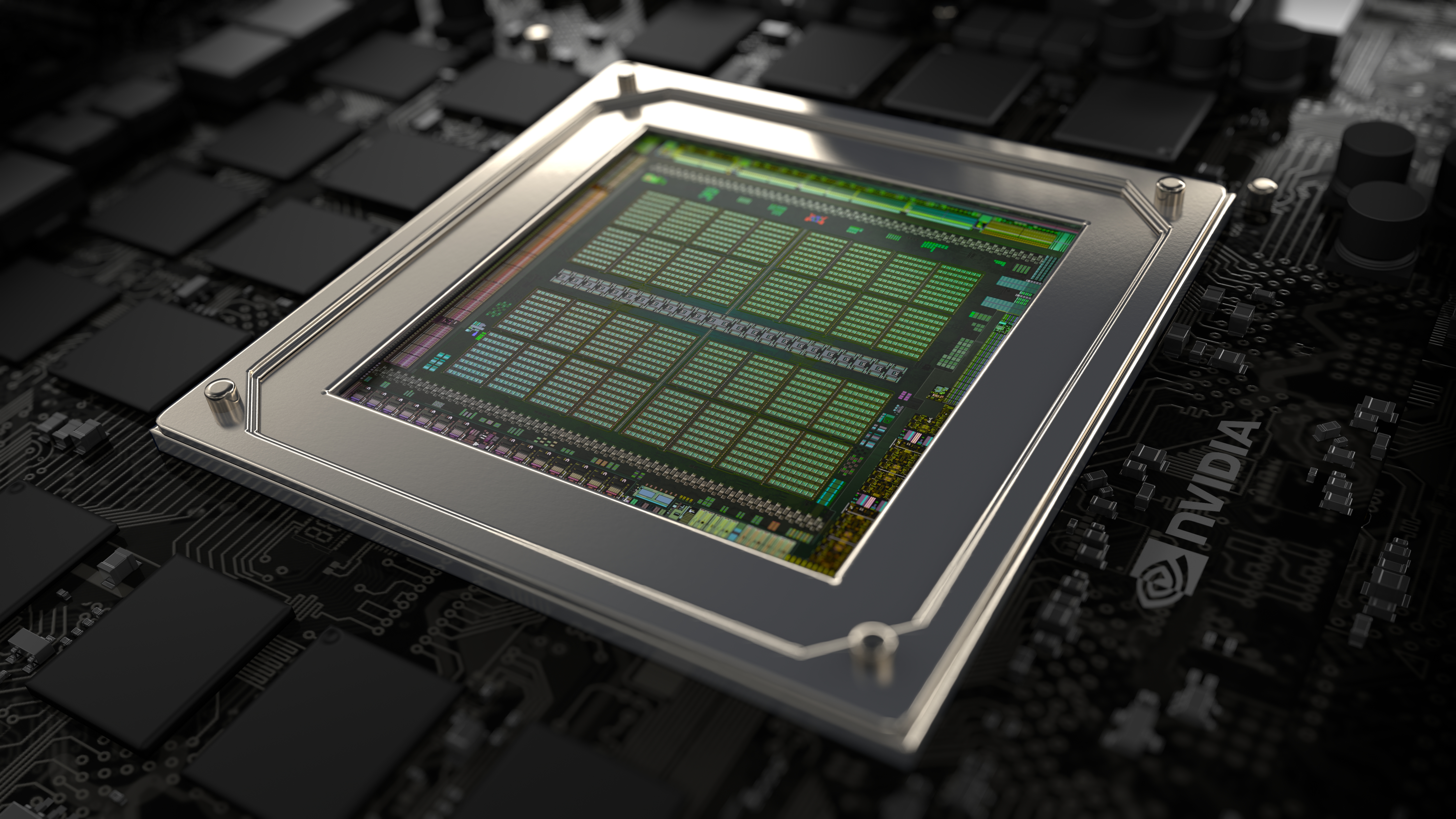
GM204 itself follows up on the GM107 with everything we loved about the first Maxwell GPUs and yet with more. “Second generation” in this case is not just a description of the second wave of Maxwell GPUs, but in fact is a technically accurate description of the Maxwell 2 architecture. As we’ll see in our deep dive into the architecture, Maxwell 2 has learned some new tricks compared to Maxwell 1 that make it an even more potent processor, and further extends the functionality of the family.
| NVIDIA GPU Specification Comparison | ||||||
| GTX 980 | GTX 970 (Corrected) | GTX 780 Ti | GTX 770 | |||
| CUDA Cores | 2048 | 1664 | 2880 | 1536 | ||
| Texture Units | 128 | 104 | 240 | 128 | ||
| ROPs | 64 | 56 | 48 | 32 | ||
| Core Clock | 1126MHz | 1050MHz | 875MHz | 1046MHz | ||
| Boost Clock | 1216MHz | 1178MHz | 928Mhz | 1085MHz | ||
| Memory Clock | 7GHz GDDR5 | 7GHz GDDR5 | 7GHz GDDR5 | 7GHz GDDR5 | ||
| Memory Bus Width | 256-bit | 256-bit | 384-bit | 256-bit | ||
| VRAM | 4GB | 4GB | 3GB | 2GB | ||
| FP64 | 1/32 FP32 | 1/32 FP32 | 1/24 FP32 | 1/24 FP32 | ||
| TDP | 165W | 145W | 250W | 230W | ||
| GPU | GM204 | GM204 | GK110 | GK104 | ||
| Transistor Count | 5.2B | 5.2B | 7.1B | 3.5B | ||
| Manufacturing Process | TSMC 28nm | TSMC 28nm | TSMC 28nm | TSMC 28nm | ||
| Launch Date | 09/18/14 | 09/18/14 | 11/07/13 | 05/30/13 | ||
| Launch Price | $549 | $329 | $699 | $399 | ||
Today’s launch will see GM204 placed into two video cards, the GeForce GTX 980 and GeForce GTX 970. We’ll dive into the specs of each in a bit, but from an NVIDIA product standpoint these two parts are the immediate successors to the GTX 780/780Ti and GTX 770 respectively. As was the case with GTX 780 and GTX 680 before it, these latest parts are designed and positioned to offer a respectable but by no means massive performance gain over the GTX 700 series. NVIDIA’s target for the upgrade market continues to be owners of cards 2-3 years old – so the GTX 600 and GTX 500 series – where the accumulation of performance and feature enhancements over the years adds up to the kind of 70%+ performance improvement most buyers are looking for.
At the very high end the GTX 980 will be unrivaled. It is roughly 10% faster than GTX 780 Ti and consumes almost 1/3rd less power for that performance. This is enough to keep the single-GPU performance crown solidly in NVIDIA’s hands, maintaining a 10-20% lead over AMD’s flagship Radeon R9 290X. Meanwhile GTX 970 should fare similarly as well, however as our sample is having compatibility issues that we haven’t been able to resolve in time, that is a discussion we will need to have another day.
NVIDIA will be placing the MSRP on the GTX 980 at $549 and the GTX 970 at $329. Depending on what you’re using as a baseline, this is either a $50 increase over the last price of the GTX 780 and launch price of the GTX 680, or a roughly $100 price cut compared to the launch prices of the GTX 780 and GTX 780 Ti. Meanwhile GTX 970 is effectively a drop-in replacement for GTX 770, launching at the price that GTX 770 has held for so long. We should see both GPUs at the usual places, though at present neither Newegg nor Amazon is showing any inventory yet – likely thanks to the odd time of launch as this coincides with NVIDIA's Game24 event – but you can check on GTX 980 and GTX 970 tomorrow.
| Fall 2014 GPU Pricing Comparison | |||||
| AMD | Price | NVIDIA | |||
| Radeon R9 295X2 | $1000 | ||||
| $550 | GeForce GTX 980 | ||||
| Radeon R9 290X | $500 | ||||
| Radeon R9 290 | $400 | ||||
| $330 | GeForce GTX 970 | ||||
| Radeon R9 280X | $280 | ||||
| Radeon R9 285 | $250 | ||||
| Radeon R9 280 | $220 | GeForce GTX 760 | |||
Finally, on a housekeeping note today’s article will be part of a series of articles on the GTX 980 series. As NVIDIA has only given us about half a week to look at GTX 980, we are splitting up our coverage to work within the time constraints. Today we will be covering GTX 980 and the Maxwell 2 architecture, including its construction, features, and the resulting GM204 GPU. Next week we will be looking at GTX 980 SLI performance, PCIe bandwidth, and a deeper look at the image quality aspects of NVIDIA’s newest anti-aliasing technologies, Dynamic Super Resolution and Multi-Frame sampled Anti-Aliasing. Finally, we will also be taking a look at the GTX 970 next week once we have a compatible sample. So stay tuned for the rest of our coverage on the Maxwell 2 family.


274 Comments
View All Comments
hojnikb - Friday, September 19, 2014 - link
7950 (which was then rebranded to 280) had 200W. With 280, they obviously upped the TDP for longer turbo speeds.ArtForz - Saturday, September 20, 2014 - link
Wasn't the 280 more of a rebranded 7950 boost (925 turbo), and not a 7950 (825, no turbo at all)?Mr Perfect - Friday, September 19, 2014 - link
True, but the 285 didn't live up to the 180 watt claim. Later in the article they showed it saving only 13 watts under load when compared to the 280. So more like 237 watts?http://www.anandtech.com/show/8460/amd-radeon-r9-2...
Which was really quite disappointing. I need something to cram in my mITX rig, and it has to be close to the 150 watts of the 6870 in there now.
Samus - Friday, September 19, 2014 - link
On a per-watt scale, AMD's GPU's are now as inefficient as their CPU's when compared to the competition. It's good they got those console contracts, because they probably won't be getting the next round if this keeps up.Absolutely amazing Maxwell is twice as efficient per watt as GCN 1.2
Laststop311 - Friday, September 19, 2014 - link
well looks like the gtx 970 is calling your name thenAlexvrb - Saturday, September 20, 2014 - link
That seems to depend on the design reviewed. THG tested a similarly clocked card by a different manufacturer and there was a much larger gap between the 280 and 285 in terms of power consumption.With that being said the 980 and 970 are both extremely fast and power efficient. Especially the 970 - if it really hits the market at around that pricing wow! Incredible value.
Strange that the 980 throttles so much at stock settings even outside of Furmark, first thing I'd do is go into the settings and fiddle a bit until it boosts consistently. But given its performance and it's not really a problem, and it can be remedied. Still, something to keep in mind especially when overclocking. I wonder how the 980 would have done with the beefier cooler from its higher-TDP predecessors, and some mild overvolting?
Laststop311 - Sunday, September 21, 2014 - link
If you look in the gaming benchmarks the gpu is hitting 80C. Nvidia's design does not allow the gpu to exceed 80C so it has to lower frequencies to stay at 80C. This is the consequence of using the titan blower cooler but removing the vapor chamber lowering its cooling capability. That's why I don't get why all these people are rushing to buy the reference design gtx 980's as they are all sold out. They are throttling by hundreds of mhz because the titan blower cooler without a vapor chamber sucks. Custom cooling options are going to make the gtx 980 able to reliably hit 1300-1400 mhz some probably even 1500 mhz under full load and still stay under the 80C limit. Keep an eye out for MSI's twin frozr V design. It's going to have a beefy radiator with 2x 100mm fans in an open air design allowing WAY more cooling potential then the reference design. The twin frozr V design should allow the card to OC and actually keep those OC frequencies under heavy load unlike the reference card which cant even keep up with its stock setting under intense gaming. We should see a pretty big performance jump going to custom coolers and the reference performance is already staggeringAlexvrb - Sunday, September 21, 2014 - link
Reviewers and "tech enthusiasts" alike jumped all over AMD when they didn't adequately cool their 290 cards. So while I don't disagree with what you're saying, I am just surprised that they would let it ship with such heavy throttling on ordinary games. Especially given that in this case it isn't because Nvidia shipped with a cooler that isn't sufficient - rather it's because by default the fan is running too slowly. Even without the vapor chamber, I bet it would be fine if they just turned up the fan just a hair. Not enough to make it loud, but enough to bring it in line with some of the other high-end cards here (under a load).Anyway I suspect the vapor chamber will return in a higher-end "980 Ti" type configuration. In the meantime, yeah I'd keep an eye out for high-end aftermarket designs with a more aggressive power delivery system and wicked cooling. There's no doubt these chips have serious potential! I'd bet an aggressive 970 could hit the market for under $400 with 980-like performance and a factory warranty. :D
I'd say "poor AMD" but this kind of leapfrogging is nothing new. Even if AMD can't come out with something really impressive in the next several months, they can always remain competitive by dropping prices. My GPU is idle outside of gaming so the actual difference in power consumption in terms of dollars is tiny. Now, for number-crunching rigs that run their GPUs 24/7... that's a different story altogether. But then again, AMD's professional cards have good DP numbers so it's kind of a wash.
Hixbot - Monday, September 22, 2014 - link
I'm very disappointed they got rid of the vapor chamber. I'm not a fan of the 3rd party coolers as they exhaust the air into the case (big deal for small form factor PCs). I prefer the blower cooler even though they are noisier, the loss of the vapor chamber is a big deal.Viewgamer - Friday, September 19, 2014 - link
LOL people screaming at the 285. It actually consumes less power than the 980 and 970 not more.Nvidia greatly understated the TDP of the 980 and 970 to put it lightly.
Both cards consume more power than the 250W TDP 7970 Ghz yet they're somehow rated at 165W and 145W how laughable !
http://i.imgur.com/nfueVP7.png