Intel’s Core M Strategy: CPU Specifications for 9mm Fanless Tablets and 2-in-1 Devices
by Ian Cutress on September 5, 2014 11:30 AM EST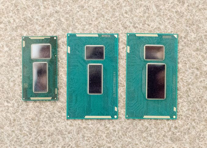
Continuing our coverage of Intel’s 14nm Technology, another series of press events held by Intel filled out some of the missing details behind the strategy of their Core M platform. Core M is the moniker for what will be the Broadwell-Y series of processors, following on from Haswell-Y, and it will be the first release of Intel’s 14nm technology. The drive to smaller, low powered fanless devices that still deliver a full x86 platform as well as the performance beyond that of a smartphone or tablet is starting to become a reality. Even reducing the size of the CPU package in all dimensions to allow for smaller devices, including reducing the z-height from 1.5mm to 1.05 mm is part of Intel’s solution, giving a total die area 37% smaller than Haswell-Y.

The first wave of three Core M parts will all be dual core flavors, with HD 5300 graphics and all within a 4.5W TDP. For Core M Intel is no longer quoting the SDP terminology due to the new design.
| Intel Core M Specifications | |||
| Core M-5Y70 | Core M-5Y10a | Core M-5Y10 | |
| Cores / Threads | 2 / 4 | 2 / 4 | 2 / 4 |
| Base Frequency / MHz | 1100 | 800 | 800 |
| Turbo Frequency / MHz | 2600 | 2000 | 2000 |
| Processor Graphics | HD 5300 | HD 5300 | HD 5300 |
| IGP Base Frequency / MHz | 100 | 100 | 100 |
| IGP Turbo Frequency / MHz | 850 | 800 | 800 |
| L3 Cache | 4 MB | 4 MB | 4 MB |
| TDP | 4.5 W | 4.5 W | 4.5 W |
| LPDDR3/DDR3L Support | 1600 MHz | 1600 MHz | 1600 MHz |
| Intel vPro | Yes | No | No |
| Intel TXT | Yes | No | No |
| Intel VT-d/VT-x | Yes | Yes | Yes |
| Intel AES-NI | Yes | Yes | Yes |
The top of the line processor will be called the Core M-5Y70, which is a bit of a mouthful but the name breaks down similarly to Intel’s main Core series. ‘5’ is similar to i5, giving us a dual-core processor with Hyper-Threading; ‘Y’ is for Broadwell-Y; and ‘70’ gives its position in the hardware stack.
The CPU will leverage both processor graphics and CPU Turbo Boost, allowing each of them to turbo at different times and different rates depending on the workload and overall power usage. Of particulary interest is that the 5Y70 features a base clock of 1.1 GHz, with turbo for both single-core and dual-core use listed as up to 2.6 GHz. The new HD 5300 GPU similarly has a 100 MHz base frequency with an 850 MHz turbo. The 5Y70 is different from the other two models in both clock speeds and features, as it will be part of Intel’s vPro program and also supports Intel TXT.
The other two processors in the stack are the 5Y10a and 5Y10, with dual-core + HT configurations and 800 MHz base frequency with turbo up to 2.0 GHz. There doesn't appear to be any major difference between the two parts, though Intel's presentation notes that the 5Y10 supports "4W Config Down TDP" (cTDP Down). The graphics is clocked slightly lower on the turbo, giving 800 MHz.
It's interesting to note that Intel informed us that the 1k unit pricing will be the same for all three processors: $281. Obviously these chips are going to end up in hybrids, tablets, and laptops that come pre-built, so the actual pricing will vary by OEM and whatever deals they have with Intel. But in general, Intel seems to be saying that OEMs can choose any of the three chips based on their power/thermal targets.
The HD Graphics 5300 is the new processor graphics and as part of the brief behind Core-M, a die shot was supplied with the important areas marked:
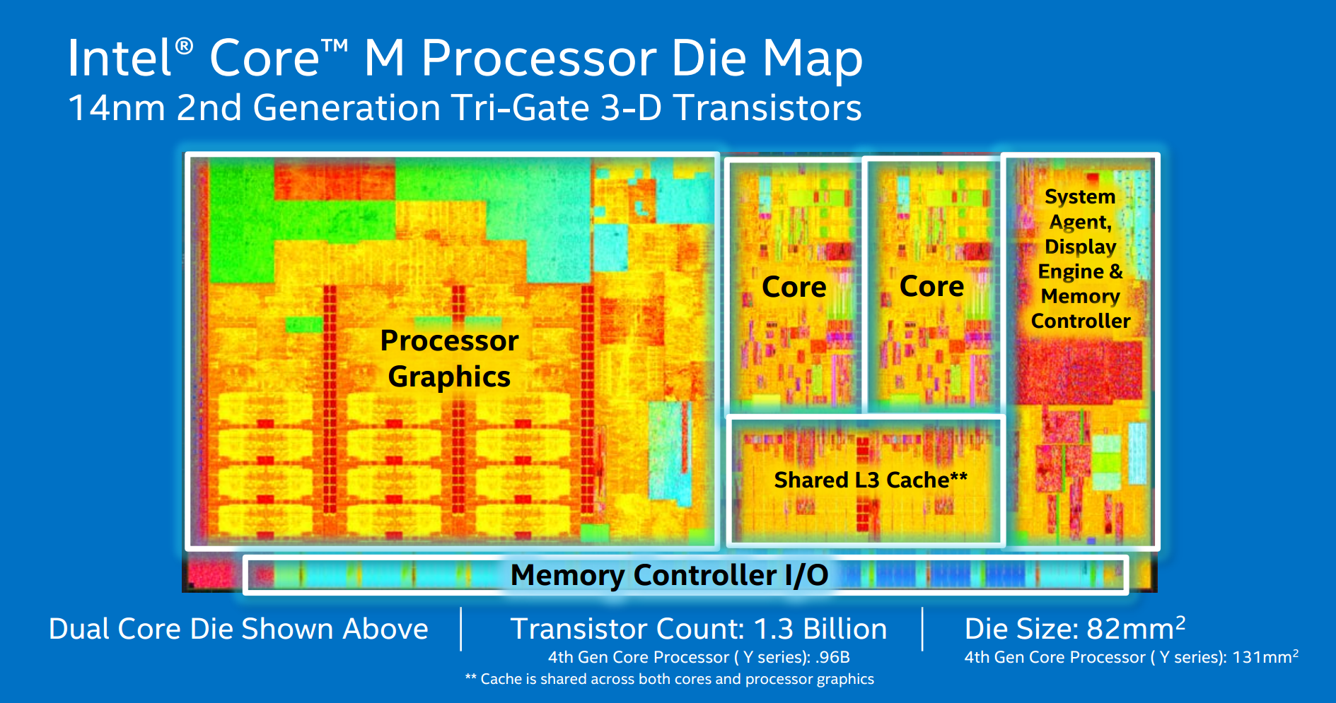
In the processor graphics section in the shot above, there clearly looks like 12 repeated units, with each representing two EUs (Execution Units). In our dive into the architecture in early August, it was stated that the minimum configuration here would be as a result of Broadwell taking 8 EUs per sub-slice, with the minimum configuration being three sub-slices, making 24 in total. This comes in combination with an increase in the L1 cache and samplers relative to the number of EUs, allowing for 25% more sampling throughput per EU.
| Intel's Tick-Tock Cadence | |||||
| Microarchitecture | Process Node | Tick or Tock | Release Year | ||
| Conroe/Merom | 65nm | Tock | 2006 | ||
| Penryn | 45nm | Tick | 2007 | ||
| Nehalem | 45nm | Tock | 2008 | ||
| Westmere | 32nm | Tick | 2010 | ||
| Sandy Bridge | 32nm | Tock | 2011 | ||
| Ivy Bridge | 22nm | Tick | 2012 | ||
| Haswell | 22nm | Tock | 2013 | ||
| Broadwell | 14nm | Tick | 2014 | ||
| Skylake | 14nm | Tock | 2015 | ||
The fundamental architecture of the GPU does not change from Haswell, albeit on a smaller process node. The GPU is confirmed as supporting DirectX 11.2, OpenGL 4.2 and OpenCL 2.0, with UltraHD (3840x2160) supported at 24 Hz through HDMI. This opens up possibilities of fanless tablets with UHD panels.

One of the main graphs Intel was pushing in their briefing was this one, indicating what power is required for a fanless tablet:
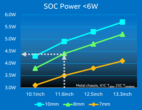
For a chassis of 7, 8 or 10mm, to have a maximum skin temperature of 41C at load, the above TDPs are required depending on the chassis size in order to go fanless. The first batch of 4.5W Core M processors aim at either the 11.6-inch, 8mm thick fanless tablet design as indicated in the graph above, or similarly a 10.1-inch 10mm thick tablet will also be suitable. Intel wants Core M to have a range of possible TDPs based on increasing or decreasing the frequency as required for a thin fanless tablet.
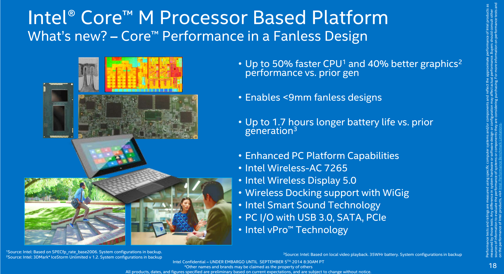
Intel is going to support extended docking functionality, especially with its business partners to allow features such as WiGig and additional I/O. Intel is also bringing a new 802.11ac design in the form of AC 7265, a lower powered version of the 2T2R 7260 for tablets. This will also support WiDi 5.0, and overall the platform aims to offer 1.7 hours longer battery life. Intel got to this ‘+1.7’ hour number with a reference design compared to a clocked-down Haswell-Y. I would like to point out that despite these numbers, a clocked-down part usually represents moving outside the optimal efficiency window, especially when dealing with low powered tablets.
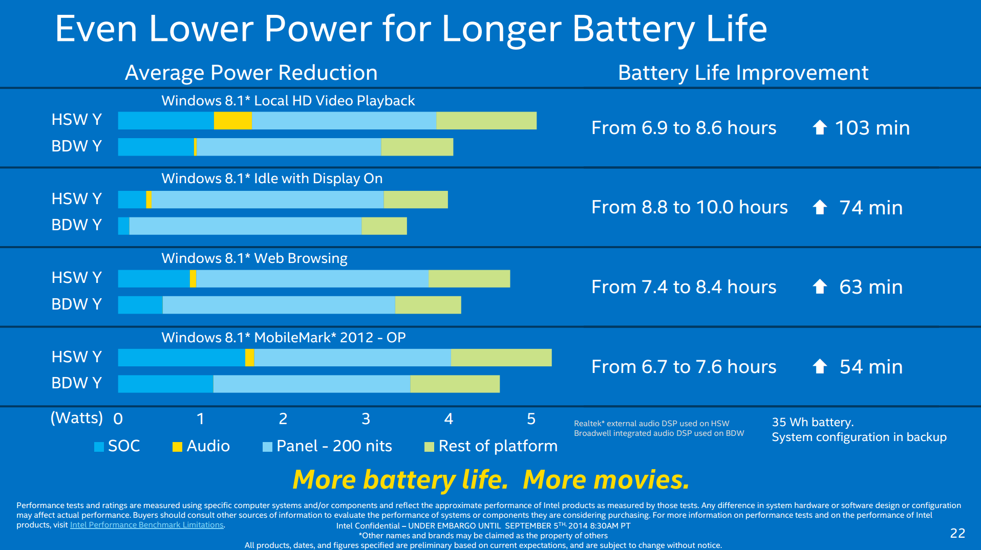
Intel used the above slide in their presentations and drew particular attention to the power consumption of the audio during HD video playback (the orange bar on the top comparison). As part of Core M, Intel is reducing power consumption of the audio segment of the system from 100s of milliwatts down to single-digit milliwatts by integrating an audio digital signaling processor (DSP) onto the die. This is what Intel refers to as its Smart Sound Technology, and is designed to shift the majority of the audio processing onto a configured part of the die which can process at lower power.
If you think you’ve heard of something like this before, you have: AMD’s TrueAudio sounds remarkably similar in its implementation and its promotion. We asked Intel if this new DSP for Broadwell would have a configurable API similar to TrueAudio, however we are still waiting on an official response to this.
The platform controller hub layout was also provided, showing USB 3.0 support along with SATA 6 Gbps and four lanes of PCIe:
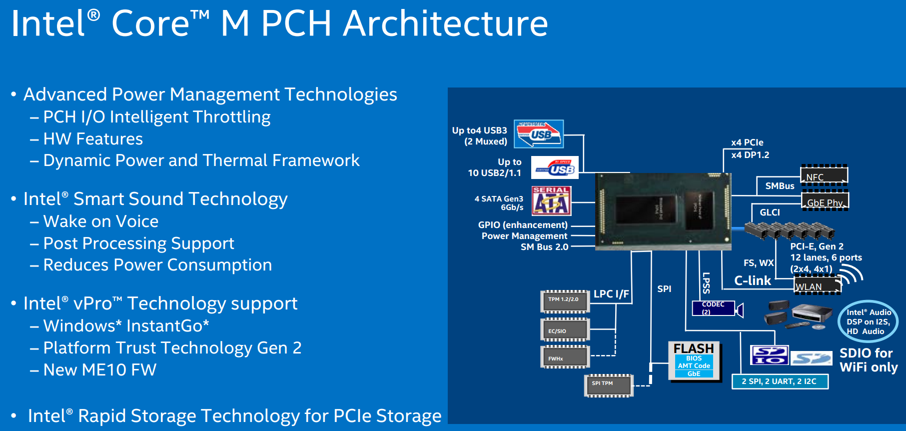
The PCH is also designed to be dynamic with power, meaning that disabling features on a design could yield a better-than-expected increase in battery life. The design will support NFC, and it is worth noting that the two USB 3.0 ports are in a mux configuration which may limit bandwidth. With a number of PCIe lanes in tow however, there are a number of controllers that could be used to expand functionality in a design.
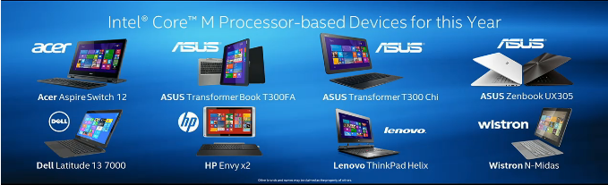
Intel will be showing off the Core M at IFA in Berlin this week, with over 20 designs based on Core M from OEMs in the known pipeline – including designs like ASUS’ Transformer Book T300 Chi announced back at Computex. The T300 Chi was specified as a 12.5-inch fanless tablet in a 7.3mm thickness design, with LTE support and a 2560x1600 display. With the 12.5-inch size and 7.3mm width, it sounds like the T300 Chi will be modifying the Core M CPU to be around 4W in order to keep the 41C skin temperature as a maximum. Intel also listed the following Core M devices at IFA:
The CPUs will be in volume production before the end of the year (we seem to have differing reports whether volume production has started already or is just about to), with systems from ~5 OEMs available in Q4, starting in late October. Intel lists both consumer and business designs for this timeframe, however volume production is expected in Q1 2015.


115 Comments
View All Comments
Kevin G - Monday, September 8, 2014 - link
We've already seen what impact a faster divisor has in real world scenarios. The change in the division unit was one of the alternations between Conroe and Wolfdale cores. In normal workloads this had less than a 1% impact in performance as division and square root are rarely used.Drumsticks - Saturday, September 6, 2014 - link
You realize turbo is what matters for responsiveness? My 4670k has a base clock of 3.4 GHz or whatever, but it still idles at 800 MHz.The new broadwell parts turbo past the i5 in the macbook air for instance, which I believe only turbos to 1.9.
The Von Matrices - Saturday, September 6, 2014 - link
"The top of the line processor will be called the Core M-5Y70, which is a bit of a mouthful but the name breaks down similarly to Intel’s main Core series. ‘5’ is similar to i5, giving us a dual-core processor with Hyper-Threading; ‘Y’ is for Broadwell-Y; and ‘70’ gives its position in the hardware stack"Are you sure about the "5" relating to "i5"? I thought that the use of "5" was just because Broadwell is the 5th generation of Core processors, similar to how Haswell parts begin in 4, Ivy Bridge in 3, and Sandy Bridge in 2.
M.Q.Leo - Saturday, September 6, 2014 - link
It seems so good.Krysto - Saturday, September 6, 2014 - link
800 Mhz ? That's beyond pathetic. Surely it must be a joke from Intel. But I'm not laughing, so it's a pretty bad one.Klimax - Saturday, September 6, 2014 - link
I didn't know you already got samples to test... Otherwise it is just horribly misinformed opinion. (Jumping to the conclusions...)Galatian - Saturday, September 6, 2014 - link
You keep posting here how bad the Broadwell chips are...are you an AMD or ARM employee? You have no performance figures yet you claim it's the worse chip ever.Kevin G - Monday, September 8, 2014 - link
The performance can be emulated rather well today with hardware out on the market. Broadwell is supposed to be a straight shrink of Haswell so IPC is the same. Take an unlocked Haswell Core i7, disable 2 cores, reduce the base clock to 800 Mhz, memory speed to 1600 Mhz and set the max turbo to 2 Ghz.GPU configuration is what is going to be difficult since the number of EU's and their throughput have changed. Giving the test chip's GPU a 20% boost in clock speed to compensate would give an approximation of the 20 -> 24 EU difference. The Core M's GPU should still be faster but such a test configuration could be seen as the minimal performance form the Core M.
There will be some performance differences as the IO platform is going to be different than what the Z97 offers due to power consumption concerns. How much of that translates into real world performance difference should be minimal in terms of CPU benchmarking. (Think the difference between Z87 to Z97.)
I'd also recommend altering the cooling solution as well as core voltages to further emulate the mobile environment. With desktop cooling, I'd expect this example to run the CPU at 2 Ghz virtually all the time but I'd still benchmark it as a reference point alongside the default desktop config. Note the power draw difference between these two and then reduce cooling capacity accordingly and keep going down until the 2.0 Ghz speed is truly a turbo setting but 800 Mhz is not throttled at all.
Krysto - Saturday, September 6, 2014 - link
I'd like to see a direct comparison between Haswell M and "Core M" Broadwell Y, that they're trying to push for mainstream. I bet Haswell M is 50-100 percent faster than "Core M".Whatever you do, Anandtech, do not - I repeat - DO NOT, compare it to Haswell Y, which is a chip so pathetic, no OEM wanted to use it this past generation. But that's what Intel will want you to do, so they can claim "performance improvements over the last generation".
But that would be an extremely misleading thing to do, since the last generation we had Haswell U as mainstream (which was quite weak, too, compared to previous generations), not Haswell Y, and before that we had SNB and IVB M, not U.
OrphanageExplosion - Saturday, September 6, 2014 - link
I agree - the comparison should be with Haswell-U, assuming that Broadwell-Y is indeed meant for two-in-ones like the Asus Transformer Chi T300 and a supposed replacement for the U chip in the MacBook Air.Haswell-Y was pretty awful, severely throttled - and Anand's SP3 Core i3 piece suggested that the battery savings were minimal there anyway on anything other than the most basic of workloads.