AMD Radeon R9 285 Review: Feat. Sapphire R9 285 Dual-X OC
by Ryan Smith on September 10, 2014 2:00 PM ESTGCN 1.2: Geometry Performance & Color Compression
Instruction sets aside, Radeon R9 285 is first and foremost a graphics and gaming product, so let’s talk about what GCN 1.2 brings to the table for those use cases.
Through successive generations of GPU architectures AMD has been iterating on and improving their geometry hardware, both at the base level and in the case of geometry generated through tessellation. This has alternated between widening the geometry frontends and optimizing the underlying hardware, with the most recent update coming in the GCN 1.1 based Hawaii, which increased AMD’s geometry processor count at the high end to 4 processors and implemented some buffering enhancements.
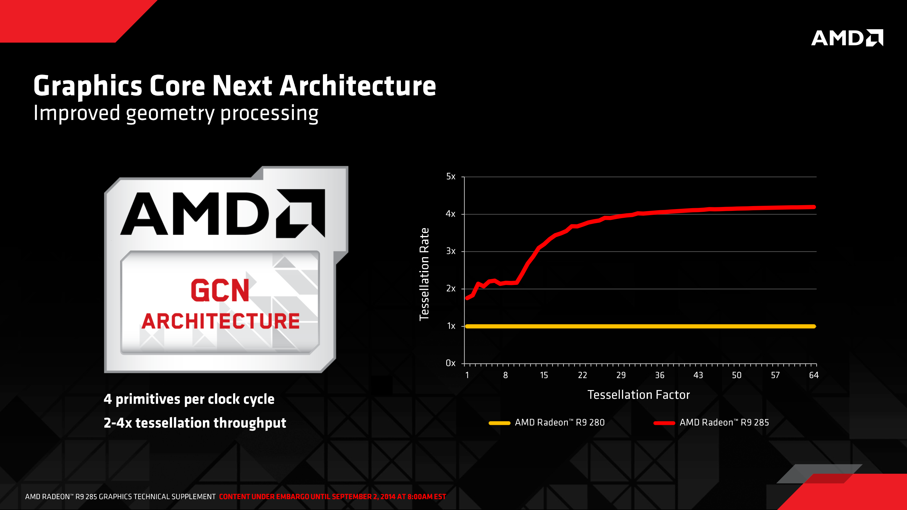

For Tonga AMD is bringing that 4-wide geometry frontend from Hawaii, which like Hawaii immediately doubles upon Tahiti’s 2-wide geometry frontend. Not stopping there however, AMD is also implementing a new round of optimizations to further improve performance. GCN 1.2’s geometry frontend includes improved vertex reuse (for better performance with small triangles) and improved work distribution between the geometry frontends to better allocate workloads between them.
At the highest level Hawaii and Tonga should be tied for geometry throughput at equivalent clockspeeds, or roughly 2x faster than Tahiti. However in practice due to these optimizations Tonga’s geometry frontend is actually faster than Hawaii’s in at least some cases, as our testing has discovered.
Comparing the R9 290 (Hawaii), R9 285 (Tonga), and R9 280 (Tahiti) in TessMark at various tessellation factors, we have found that while Tonga trails Hawaii at low tessellation factors – and oddly enough even Tahiti – at high tessellation factors the tables are turned. With x32 and x64 tessellation, the Tonga based R9 285 outperforms both cards in this raw tessellation test, and at x64 in particular completely blows away Hawaii, coming close to doubling its tessellation performance.

At the x64 tessellation factor we see the R9 285 spit out 134fps, or equivalent to roughly 1.47B polygons/second. This is as compared to 79fps (869M Polys/sec) for the R9 290, and 68fps (748M Polys/sec) for the R9 280. One of the things we noted when initially reviewing the R9 290 series was that AMD’s tessellation performance didn’t pick up much in our standard tessellation benchmark (Tessmark at x64) despite the doubling of geometry processors, and it looks like AMD has finally resolved that with GCN 1.2’s efficiency improvements. As this is a test with a ton of small triangles, it looks like we’ve hit a great case for the vertex reuse optimizations.
Meanwhile AMD’s other GCN 1.2 graphics-centric optimization comes at the opposite end of the rendering pipeline, where the ROPs and memory controllers lie. As we mentioned towards the start of this article, one of the notable changes between the R9 280 and R9 285 is that the latter utilizes a smaller 256-bit memory bus versus the R9 280’s larger 384-bit memory bus, and as a result has around 27% less memory bandwidth than the R9 280. Under most circumstances such a substantial loss in memory bandwidth would result in a significant performance hit, so for AMD to succeed Tahiti with a smaller memory bus, they needed a way to be able to offset that performance loss.
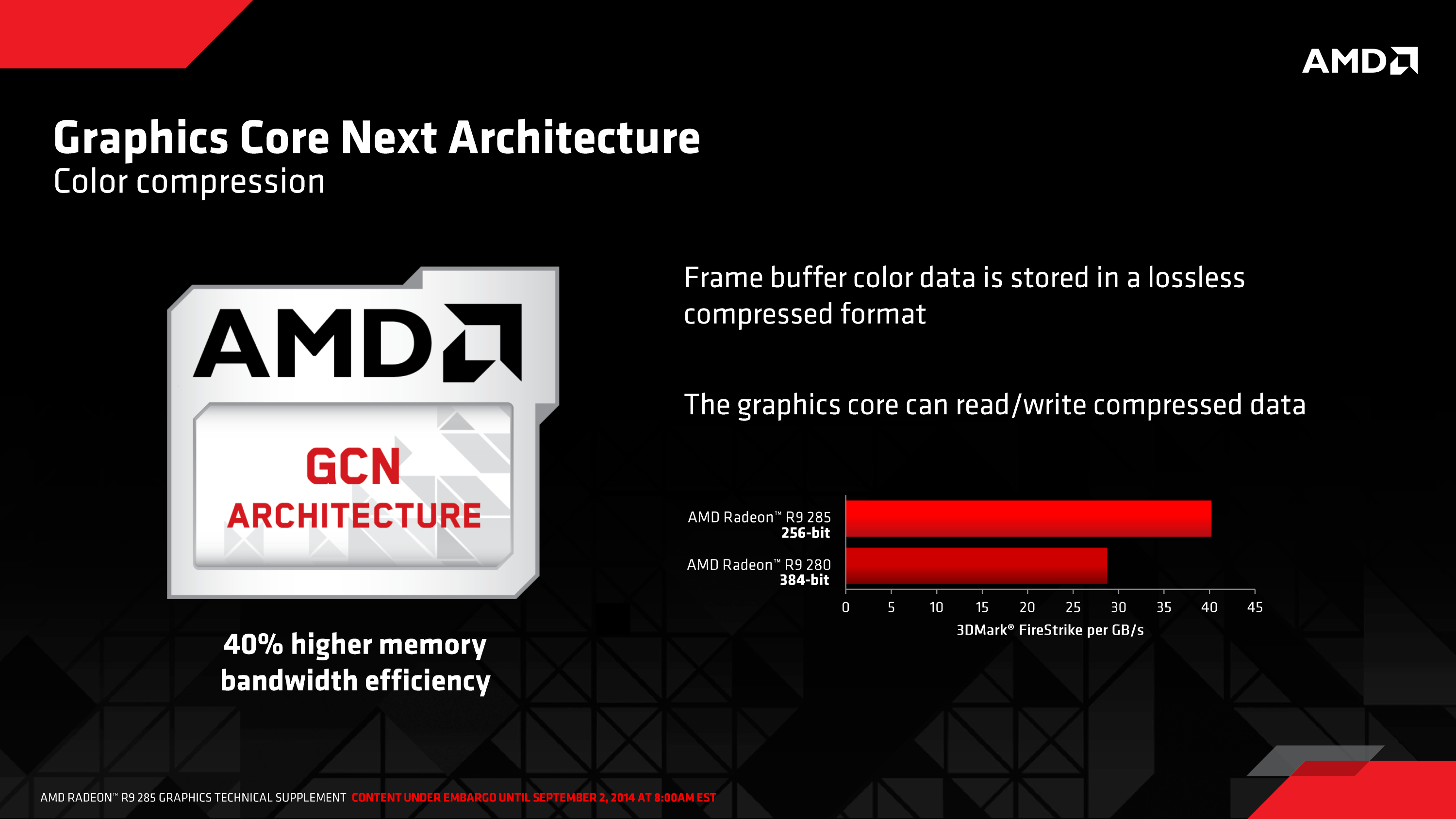
The end result is that GCN 1.2 introduces a new color compression method for its ROPs, to reduce the amount of memory bandwidth required for frame buffer operations. Color compression itself is relatively old – AMD has had color compression in some form for almost 10 years now – however GCN 1.2 iterates on this idea with a color compression method AMD is calling “lossless delta color compression.”
Since AMD is only meeting us half-way here we don’t know much more about what this does. Though the fact that they’re calling it delta compression implies that AMD has implemented a further layer of compression that works off of the changes (deltas) in frame buffers, on top of the discrete compression of the framebuffer. In this case this would not be unlike modern video compression codecs, which between keyframes will encode just the differences to reduce bandwidth requirements (though in AMD’s case in a lossless manner).
AMD’s own metrics call for a 40% gain in memory bandwidth efficiency, and if that is the average case it would more than make up for the loss of memory bandwidth from working on a narrower memory bus. We’ll see how this plays out over our individual games over the coming pages, but it’s worth noting that even our most memory bandwidth-sensitive games hold up well compared to the R9 280, never losing anywhere near the amount of performance that such a memory bandwidth reduction would imply (if they lose performance at all).


86 Comments
View All Comments
chizow - Thursday, September 11, 2014 - link
If Tonga is a referendum on Mantle, it basically proves Mantle is a failure and will never succeed. This pretty much shows most of what AMD said about Mantle is BS, that it takes LESS effort (LMAO) on the part of the devs to implement than DX.If Mantle requires both an application update (game patch) from devs AFTER the game has already run past its prime shelf-date AND also requires AMD to release optimized drivers every time a new GPU is released, then there is simply no way Mantle will ever succeed in a meaningful manner with that level of effort. Simply put, no one is going to put in that kind of work if it means re-tweaking every time a new ASIC or SKU is released. Look at BF4, its already in the rear-view mirror from DICE's standpoint, and no one even cares anymore as they are already looking toward the next Battlefield#
TiGr1982 - Thursday, September 11, 2014 - link
Please stop calling GPUs ASICs - this looks ridiculous.Please go to Wikipedia and read what "ASIC" is.
chizow - Thursday, September 11, 2014 - link
Is this a joke or are you just new to the chipmaking industry? Maybe you should try re-reading the Wikipedia entry to understand GPUs are ASICs despite their more recent GPGPU functionality. GPU makers like AMD and Nvidia have been calling their chips ASICs for decades and will continue to do so, your pedantic objections notwithstanding.But no need to take my word for it, just look at their own internal memos and job listings:
https://www.google.com/#q=intel+asic
https://www.google.com/#q=amd+asic
https://www.google.com/#q=nvidia+asic
TiGr1982 - Thursday, September 11, 2014 - link
OK, I accept your arguments, but I still don't like this kind of terminology. To me, one may call things like fixed-function video decoder "ASIC" (for example UVD blocks inside Radeon GPUs), but not GPU as a whole, because people do GPGPU for a number of years on GPUs, and "General Purpose" in GPGPU contradicts with "Aplication Specific" in ASIC, isn't it?So, overall it's a terminology/naming issue; everyone uses the naming whatever he wants to use.
chizow - Thursday, September 11, 2014 - link
I think you are over-analyzing things a bit. When you look at the entire circuit board for a particular device, you will see each main component or chip is considered an ASIC, because each one has a specific application.For example, even the CPU is an ASIC even though it handles all general processing, but its specific application for a PC mainboard is to serve as the central processing unit. Similarly, a southbridge chip handles I/O and communications with peripheral devices, Northbridge handles traffic to/from CPU and RAM and so on and so forth.
TiGr1982 - Thursday, September 11, 2014 - link
OK, then according to this (broad) understanding, every chip in silicon industry may be called ASIC :)Let it be.
chizow - Friday, September 12, 2014 - link
Yes, that is why everyone in the silicon industry calls their chips that have specific applications ASICs. ;)Something like a capacitor, or resistor etc. would not be as they are of common commodity.
Sabresiberian - Thursday, September 11, 2014 - link
I reject the notion that we should be satisfied with a slower rate of GPU performance increase. We have more use than ever before for a big jump in power. 2560x1440@144Hz. 4K@60Hz.Of course it's all good for me to say that without being a micro-architecture design engineer myself, but I think it's time for a total re-think. Or if the companies are holding anything back - bring it out now, please! :)
Stochastic - Thursday, September 11, 2014 - link
Process node shrinks are getting more and more difficult, equipment costs are rising, and the benefits of moving to a smaller node are also diminishing. So sadly I think we'll have to adjust to a more sedate pace in the industry.TiGr1982 - Thursday, September 11, 2014 - link
I'm a longstanding AMD Radeon user for more than 10 years, but after reading this R9 285 review I can't help but think that, based on results of smaller GM107 in 750 Ti, GM204 in GTX 970/980 may offer much better performance/Watt/die area (at least for gaming tasks) in comparison to the whole AMD GPU lineup. Soon we'll see whether or not this will be the case.