Intel’s 14nm Technology in Detail
by Ryan Smith on August 11, 2014 12:45 PM EST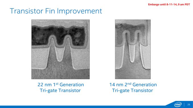
Much has been made about Intel’s 14nm process over the past year, and admittedly that is as much as Intel’s doing as it is the public’s. As one of the last Integrated Device Manufacturers and the leading semiconductor manufacturer in the world, Intel has and continues to set the pace for the semiconductor industry. Which means that Intel’s efforts to break the laws of physics roughly every 2 years mark an important milestone in the continuing development of semiconductor technology and offer a roadmap of sorts to what other semiconductor manufacturers might expect.
To that end, at a time when ramping up new process nodes is more complex and more expensive than ever, Intel’s 14nm process is especially important. Although concerns over the immediate end of Moore’s Law remain overblown and sensationalistic, there is no denying that continuing the pace of Moore’s Law has only gotten more difficult. And as the company on the forefront of semiconductor fabrication, if anyone is going to see diminishing returns on Moore’s Law first it’s going to be Intel.
Today Intel is looking to put those concerns at rest. Coinciding with today’s embargo on Intel’s 14nm technology and a preview of Intel’s upcoming Broadwell architecture based Core M processor, Intel will be holding a presentation dubbed Advancing Moore’s Law in 2014. Intel for their part is nothing short of extremely proud over what advancements they have made over the last several years to make their 14nm process a reality, and with that process now in volume production in their 14nm Oregon fab and being replicated to others around the world, Intel is finally ready to share more information about the 14nm process.
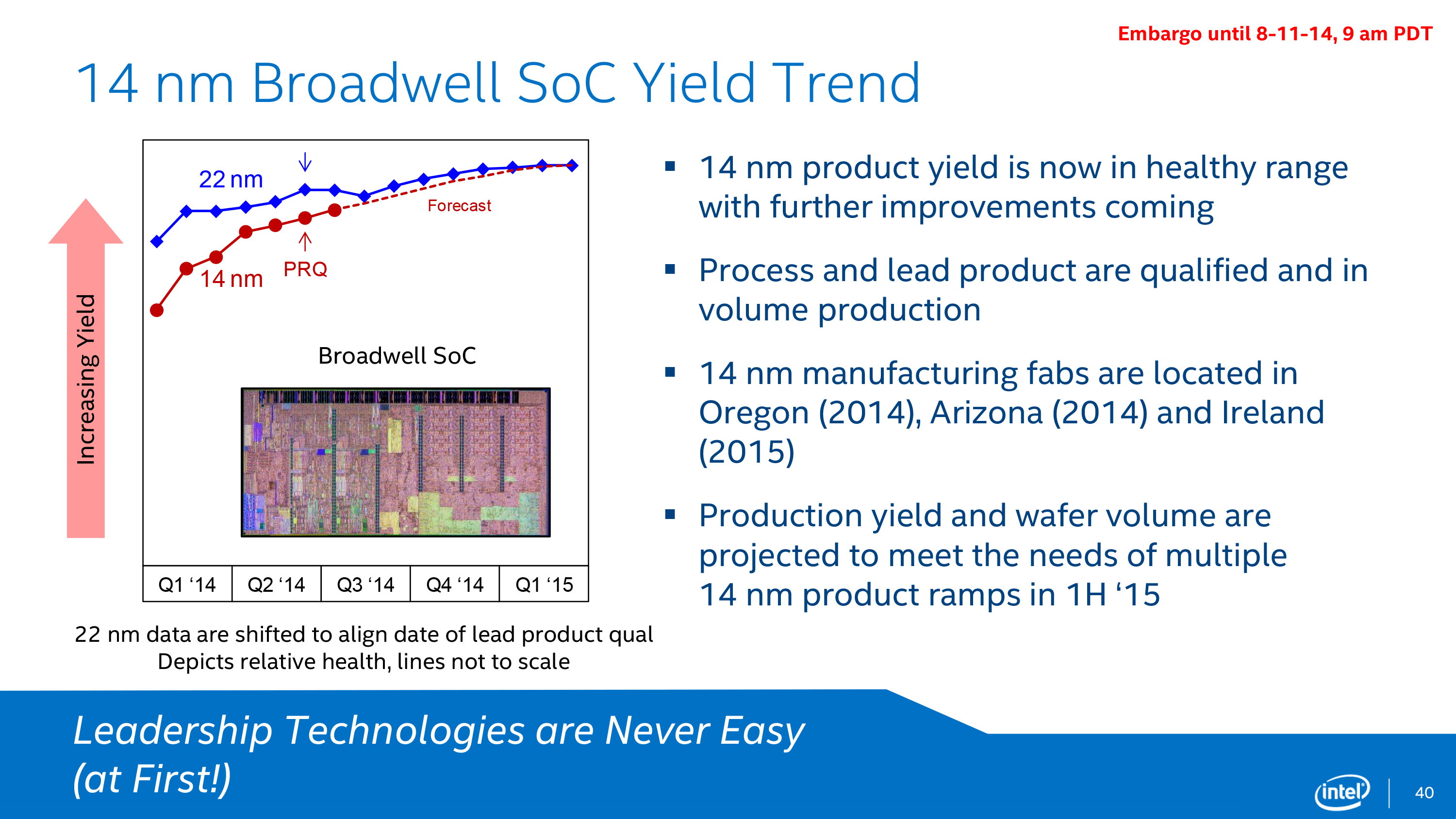
We’ll start off our look at Intel’s 14nm process with a look at Intel’s yields. Yields are important for any number of reasons, and in the case of Intel’s 14nm process the yields tell a story of their own.
Intel’s 14nm process has been their most difficult process to develop yet, a fact that Intel is being very straightforward about. Throughout the life of the 14nm process so far its yields have trailed the 22nm at equivalent points in time, and while yields are now healthy enough for volume production Intel still has further work to do to improve the process to catch up with 22nm. In fact at the present Intel’s 22nm process is the company’s highest yielding (lowest defect density) process ever, which goes to show just how big a set of shoes the up and coming 14nm process needs to fill to completely match its predecessor.
Concerns over these yields has no doubt played a part in Intel’s decision to go ahead with today’s presentation, for if nothing else they need to showcase their progress to their investors and justify the company’s heavy investment into 14nm and other R&D projects. While 14nm has made it into production in 2014 and the first 14nm products will hit retail by the end of the year, these yield issues have caused 14nm to be late for Intel. Intel’s original plans, which would have seen the bulk of their Broadwell lineup launch in 2014, have been reduced to the single Broadwell-Y SKU this year, with the rest of the Broadwell lineup launching in 2015.
Ultimately while 14nm is still catching up to 22nm, Intel is increasingly confident that they will be able to finish catching up, forecasting that 14nm will reach parity with 22nm on a time adjusted basis in the first quarter of 2015, or roughly 6 months from now. Intel is already in the process of replicating their 14nm to their other fabs, with fabs in Arizona and Ireland expected to come online later this year and in 2015 respectively. These fab ramp-ups will in turn allow Intel to further increase their manufacturing capacity, with Intel projecting that they will have sufficient volume to handle multiple 14nm product ramps in H1’2015.
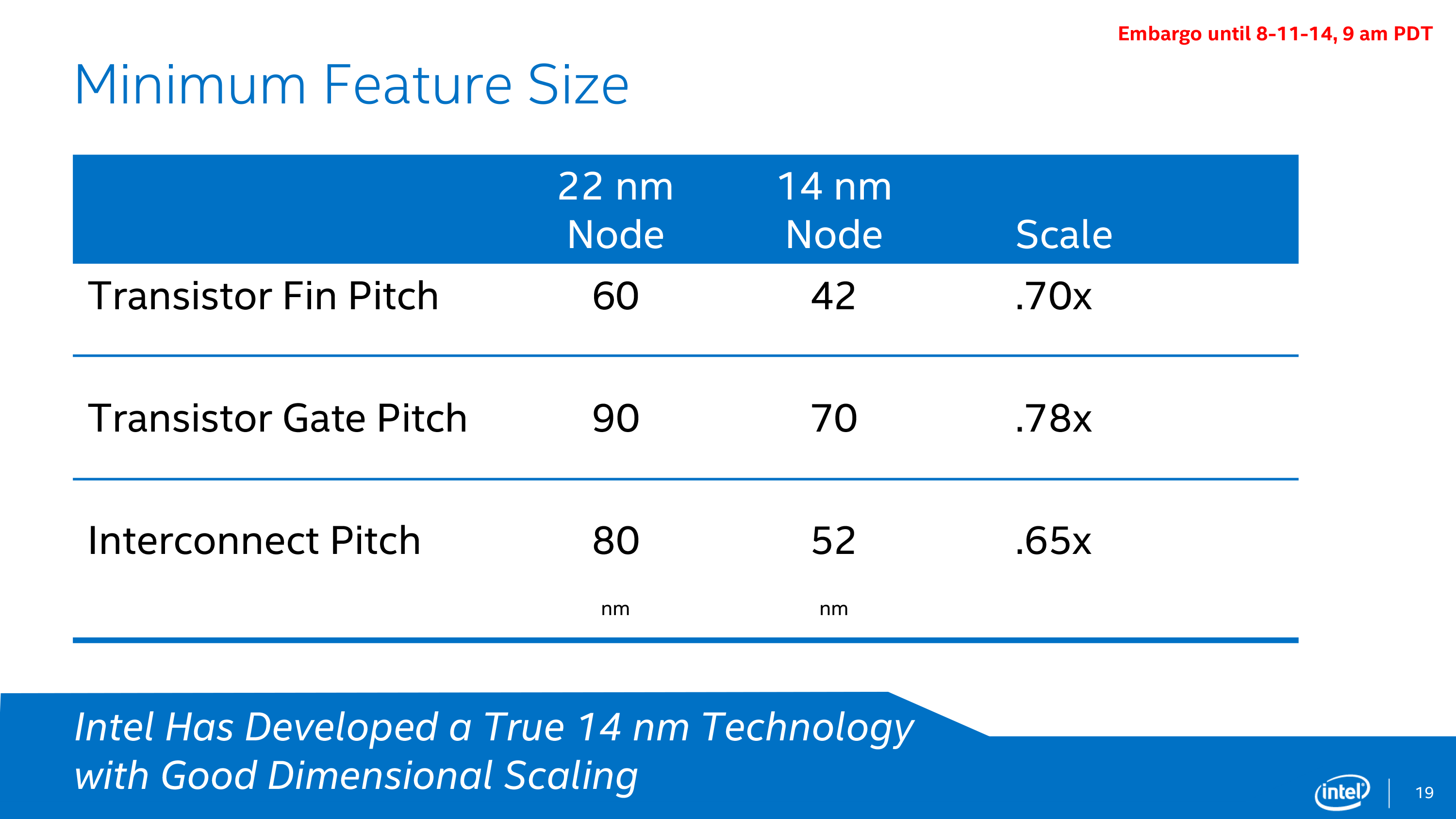
Moving on to the specifications and capabilities of their 14nm process, Intel has provided the minimum feature size data for 3 critical feature size measurements: transistor fin pitch, transistor gate pitch, and the interconnect pitch. From 22nm to 14nm these features have been reduced in size by between 22% and 35%, which is consistent with the (very roughly) 30%-35% reduction in feature size that one would expect from a full node shrink.
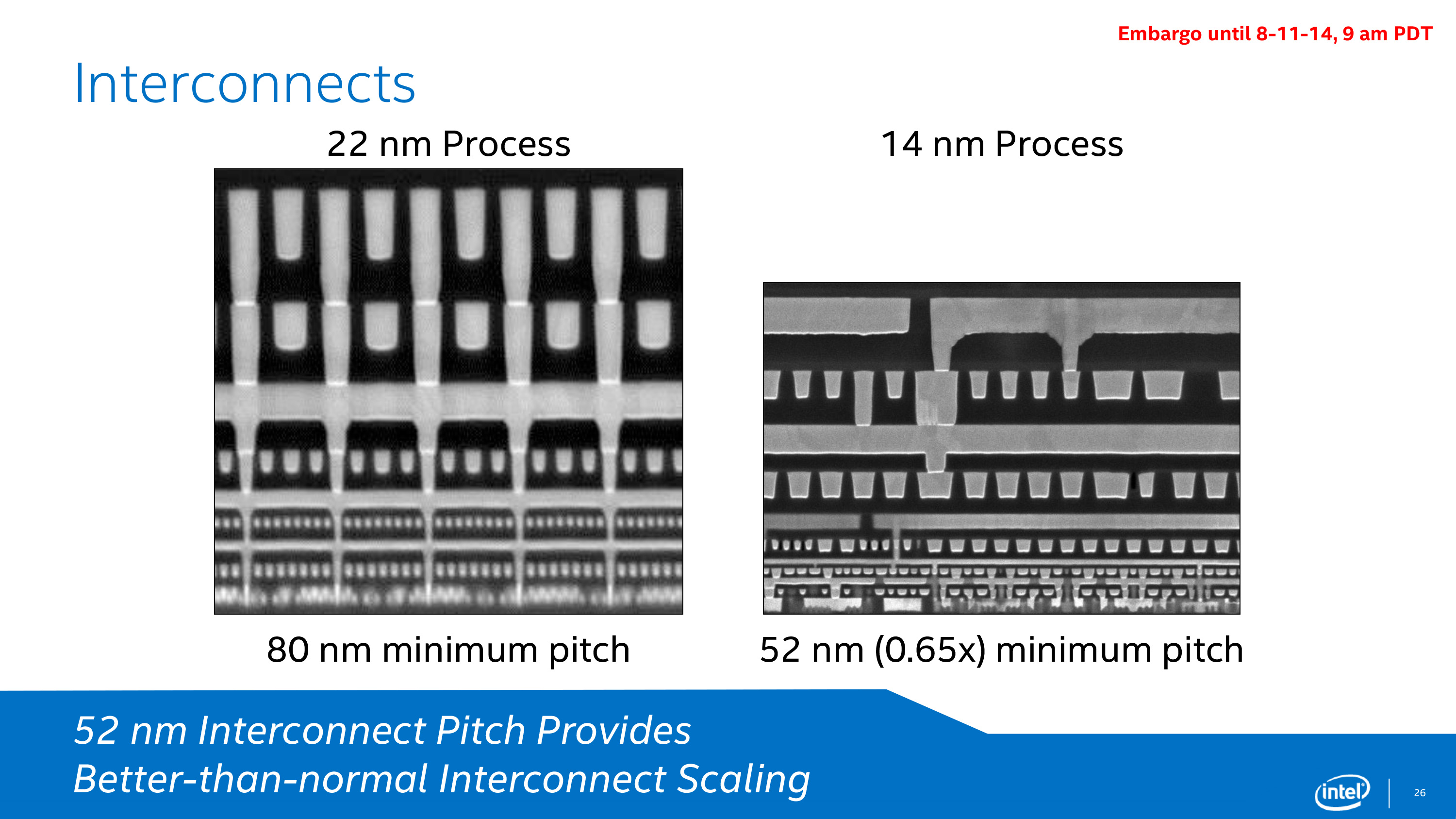
Intel is especially proud of their interconnect scaling on the 14nm node, as the 35% reduction in the minimum interconnect pitch is better than normal for a new process node.
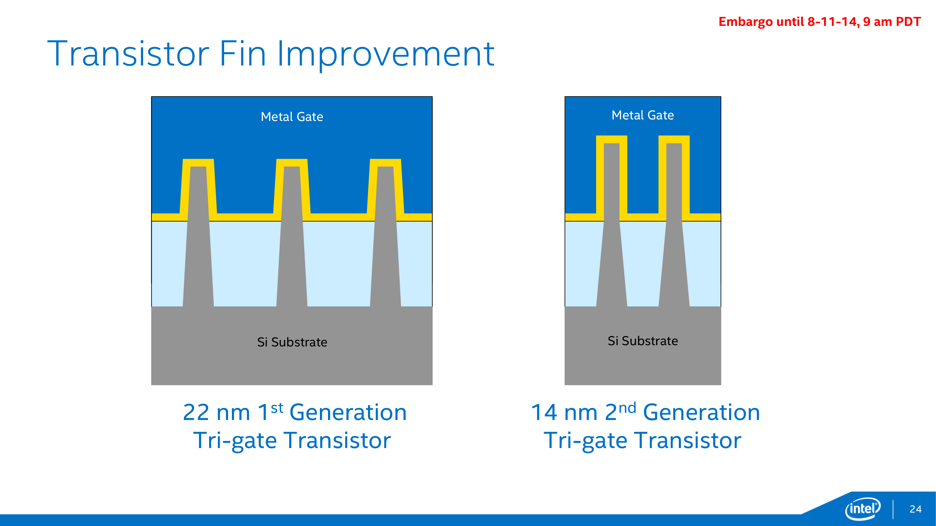
Along with the immediate feature size improvements that come with a smaller manufacturing node, Intel has also been iterating on their FinFET technology, which is now in its second generation for the 14nm process. Compared to the 22nm process, the 14nm process’s fins are more tightly packed, thinner, taller, and fewer in number (per transistor).
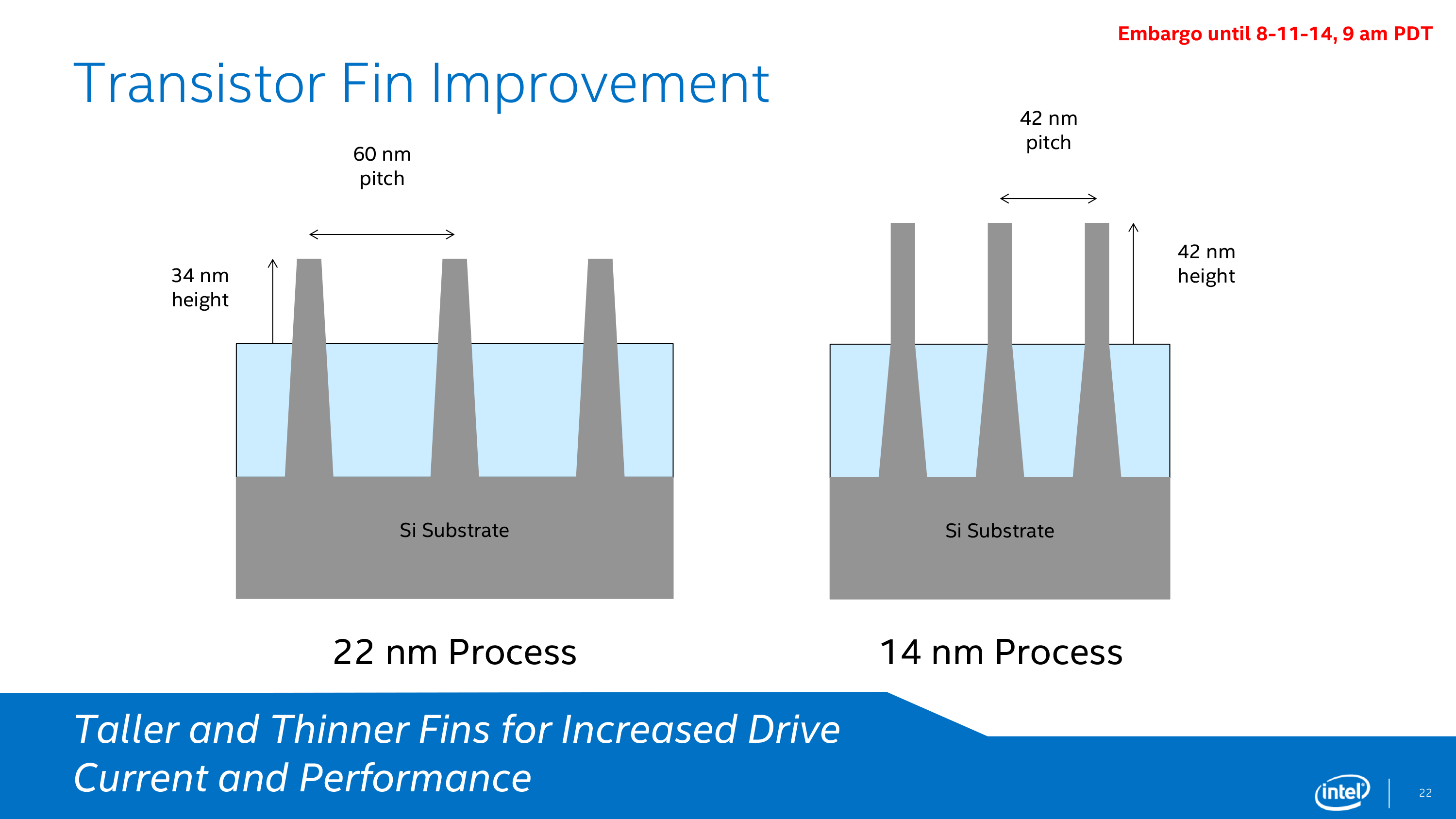
Each one of these changes in turn improves the performance of the FinFETs in some way. The tighter density goes hand-in-hand with 14nm’s feature size reductions, while the taller, thinner fins allow for increased drive current and increased performance. Meanwhile by reducing the number of fins per transistor, Intel is able to improve on density once again while also reducing the transistor capacitance that results from those fins.


Intel is also reporting that they have been able to maintain their desired pace at improving transistor switching speeds and reducing power leakage. Across the entire performance curve the 14nm process offers a continuum of better switching speeds and/or lower leakage compared to Intel’s 22nm process, which is especially important for Intel’s low power ambitions with the forthcoming Core M processor.
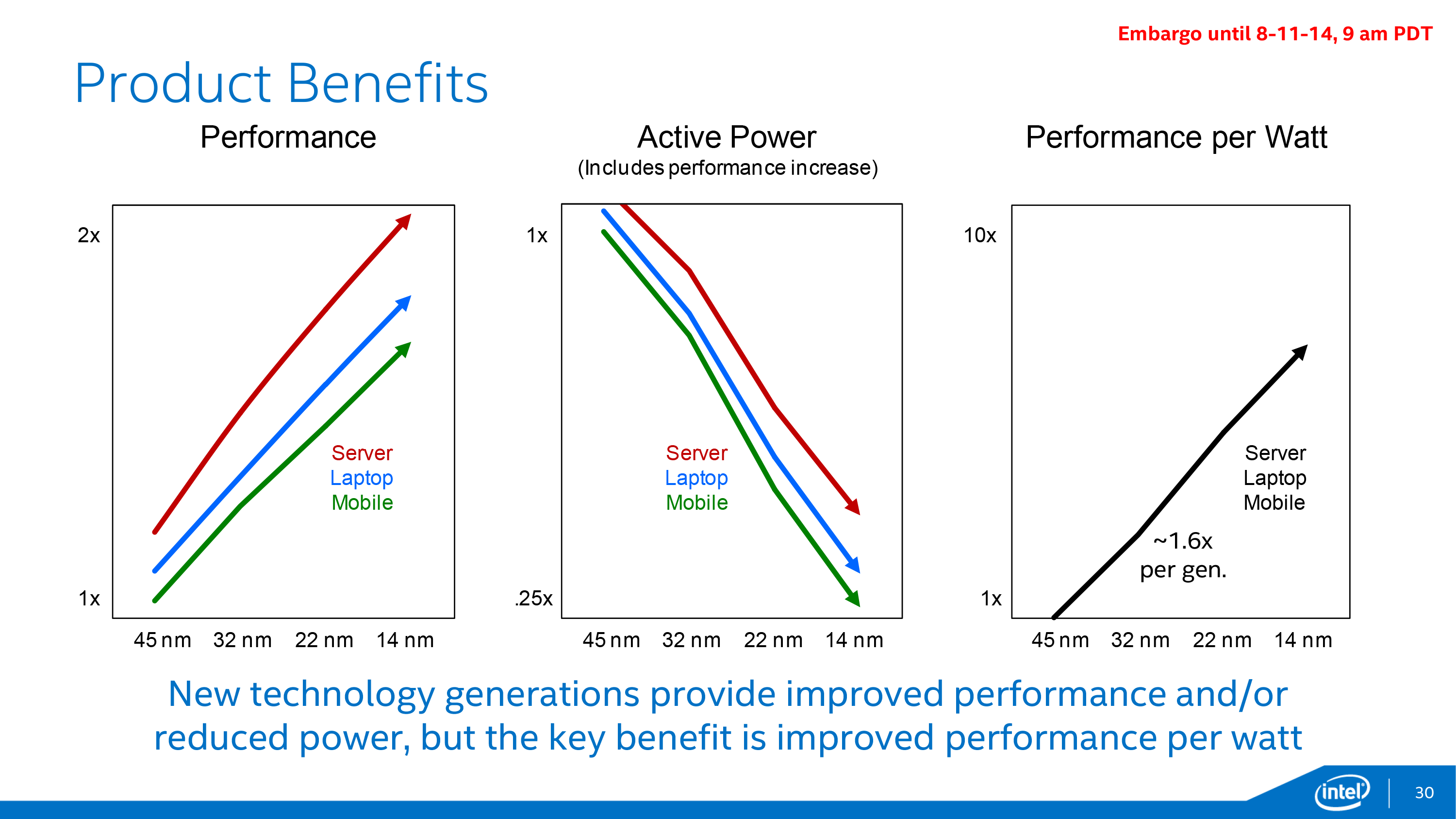
Plotted differently, here we can see how the last several generations of Intel’s process nodes compare across mobile, laptop, and server performance profiles. All 3 profiles are seeing a roughly linear increase in performance and decrease in active power consumption, which indicates that Intel’s 14nm process is behaving as expected and is offering similar gains as past processes. In this case the 14nm process should deliver a roughly 1.6x increase in performance per watt, just as past processes have too.
Furthermore, these base benefits when coupled with Intel’s customized 14nm process for Core M (Broadwell-Y) and Broadwell’s power optimizations have allowed Intel to more than double their performance per watt as compared to Haswell-Y.
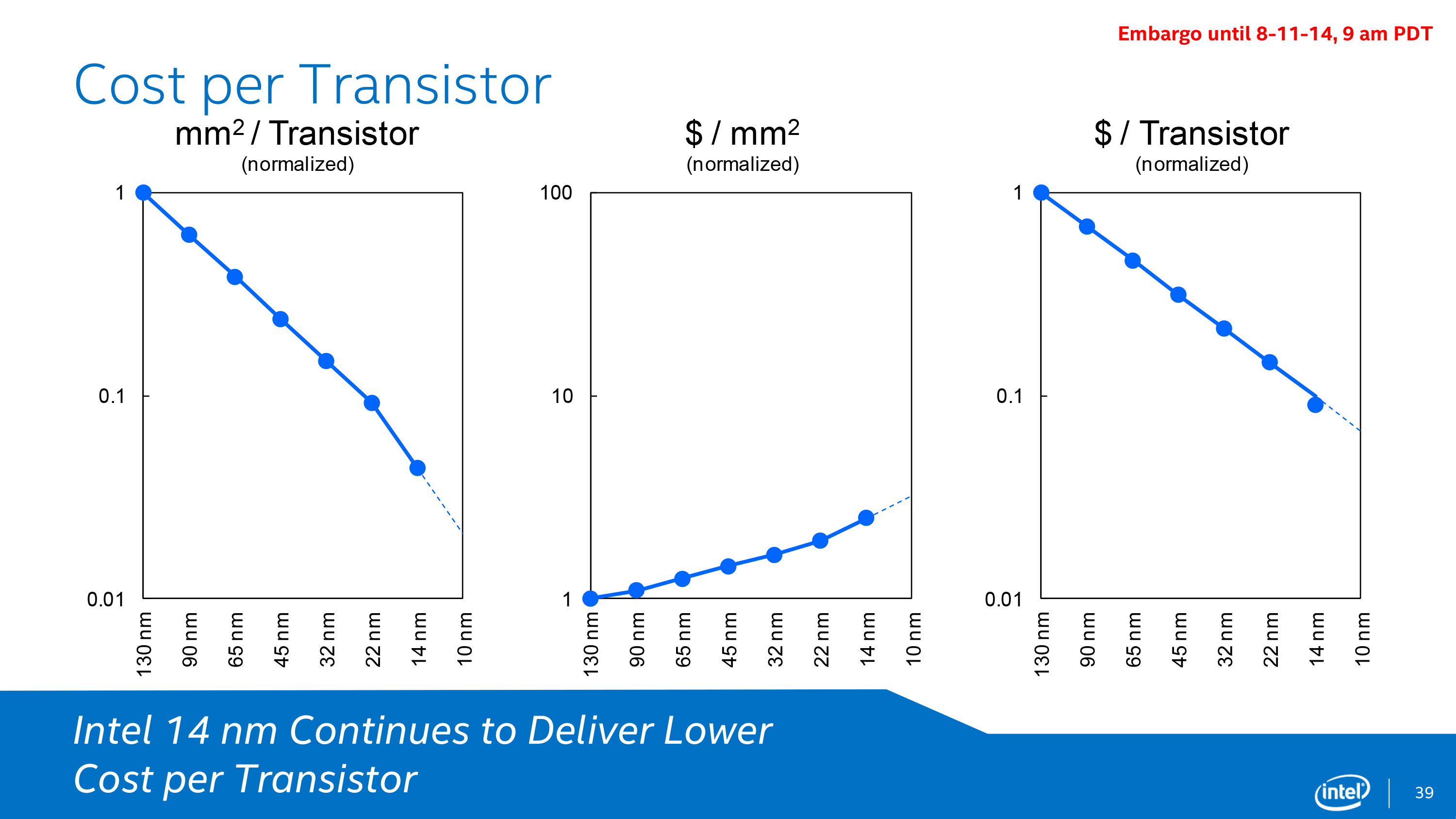
Moving on to costs, Intel offers a breakdown of costs on a cost per mm2 and pairs that with a plot of transistor sizes. By using more advanced double patterning on their 14nm node Intel was able to achieve better than normal area scaling, as we can see here. The tradeoff for that is that wafer costs continue to rise from generation to generation, as double patterning requires additional time and ever-finer tools that drive up the cost of production. The end result is that while Intel’s cost per transistor is not decreasing as quickly as the area per transistor, the cost is still decreasing and significantly so. Even with the additional wafer costs of the 14nm process, on a cost per transistor basis the 14nm process is still slightly ahead of normal for Intel.
At the same time the fact that costs per transistor continue to come down at a steady rate may be par for the course, but that Intel has been able to even maintain par for the course is actually a very significant accomplishment. As the cost of wafers and fabbing have risen over the years there has been concern that transistor costs would plateau, which would lead to chip designers being able to increase their performance but only by increasing prices, as opposed to the past 40 years of cheaper transistors allowing prices to hold steady while performance has increased. So for Intel this is a major point of pride, especially in light of complaints from NVIDIA and others in recent years that their costs on new nodes aren’t scaling nearly as well as they would like.
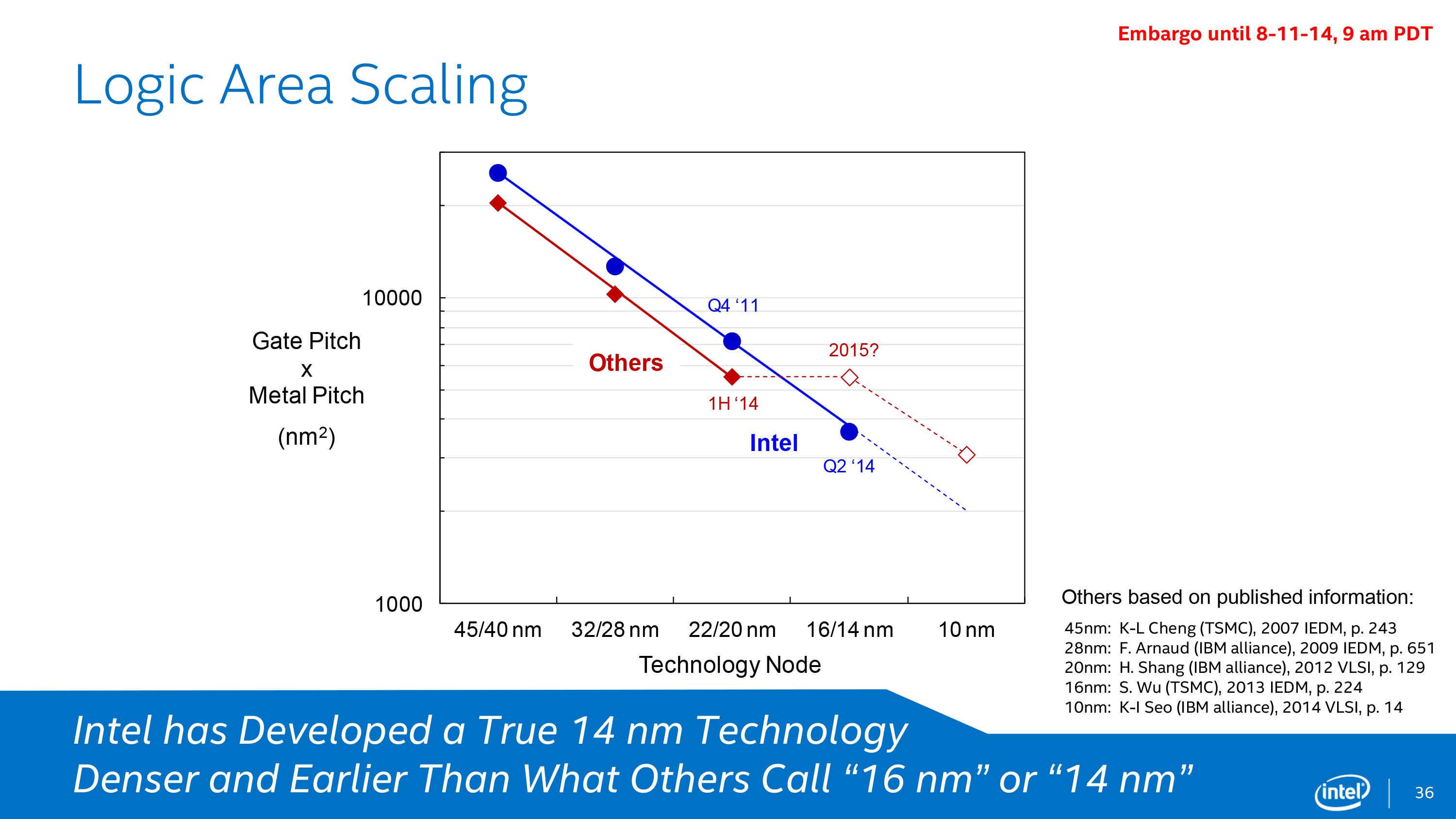
Which brings us to the final subject of Intel’s 14nm presentation, the competitive landscape. Between the ill-defined naming of new process nodes across the entire industry and Intel’s continuing lead in semiconductor manufacturing, Intel likes to point out how their manufacturing nodes compare to foundry competitors such as TSMC and the IBM alliance. Citing 3rd party journal articles for comparison, Intel claims that along with their typical lead in rolling out new nodes, as of the 14nm node they are going to have a multiple generation technical advantage. They expect that their 14nm node will offer significantly smaller feature sizes than competing 14nm nodes, allowing them to maintain consistent logic area scaling at a time when their competitors (i.e. TSMC) cannot.
From a technical perspective it's quite obvious why it is that Intel is able to maintain density scaling above the level that TSMC and Common Platform members can deliver. In short, this goes back to the improved interconnect density that was discussed earlier in this article. While Intel is pushing 14nm transistor and interconnect, TSMC and Common Platform members are using the same interconnect technology that they did at 20nm. This means that only areas where transistor density was the gating factor for 20nm will decrease in size at 14/16nm, while areas already gated by 20nm interconnect technology won't be able to get any smaller.
Thus for what it’s worth the basic facts do appear to check out, but we would be the first to point out that there is more to semiconductor manufacturing than just logic area scaling. At least until Intel’s competitors start shipping their FinFET products this is going to be speculative, and doesn’t quantify how well those competing process nodes will perform. But then again, the fact that Intel is already on their second FinFET node when their competitors are still ramping up their first is no small feat.
Wrapping things up, while Intel’s bring up of their 14nm process has not been without problems and delays, at this point Intel appears to be back on track. 14nm is in volume production in time for Broadwell-Y to reach retail before the end of the year, and Intel is far enough along that they can begin replicating the process to additional fabs for production in 2014 and 2015. Meanwhile it will still be a few months before we can test the first 14nm chips, but based on Intel’s data it looks like they have good reason to be optimistic about their process. The feature size and leakage improvements are in-line with previous genartion process nodes, which should be a great help for Intel in their quest to crack the high performance mobile market in the coming year.


38 Comments
View All Comments
nand - Wednesday, August 13, 2014 - link
multithreading is just about twice as fast for less power http://www.anandtech.com/bench/product/47?vs=1260RussianSensation - Wednesday, August 13, 2014 - link
Good comparison but less practical in the real world because i7 920 can be easily overclocked to 4-4.4Ghz. On AT, an enthusiast site, the proper comparison should really be i7 920 @ 4.0-4.2Ghz vs. i7 4790K @ 4.7-4.8Ghz. Obviously the latter would bin but nowhere near by 2x in performance and in games it would be very small. The i7 920 @ 4.2Ghz would use a heck of a lot more power though. I am looking forward to seeing what (A) 5820K OC can do on X99 and (B) how much overclocking headroom Skylake has next year on 14nm as i7 3770K and 4770K were pretty disappointing compared to 2600Ks.r3loaded - Wednesday, August 13, 2014 - link
Ahem: http://www.anandtech.com/bench/product/47?vs=1260IUU - Friday, August 15, 2014 - link
I don't think this is necessarily true.The core i7 920(I have one too), was a high end processor running at 130W. If you take into account that the only difference with i7 960 was practically the clock speed, then you realize
that the i7 920 was more like a close analogue to 4960x or 4930k than to 4820. The fact that it costs more is only relevant to the market(the fake human rules). Physically, it shows that it's possible to have twice the computing power at about the same space with about the same energy requirements, and this is only that really matters, if you want to be objective.
A 4930k or 4960x(the true high-ends of today, 4770k is high-end for those with short memory) is definitely 2x or maybe more where it matters(loads that can be multithreaded). If you say, that multithreading doesn't offer much benefit, because most programs can't take advantage of more
cores, you are practically right, and yet somewhat wrong. I mean, what is the meaning of threading in a "hello world" program? Many apps today, no matter how complex they might seem, they are "hello programs"; meaning that it would be pointless to be multithreaded even if they could.
My opinion is known.I don't think these chips have no place. We are just in a transitional period.
We still think of computing as office suits, games and media manipulation; these are the glory apps of a time past. Just wait a little and see, speech recognition, image recognition, language comprehension, and then come and tell me multicores are useless. This might not come right away, true, you should keep your money and buy when you have the biggest benefit; but it doesn't mean that progress has stopped for the slightest, market availability has shrinked instead.
Maybe they actually reach a dead end after some years, but they haven't, yet...
nissangtr786 - Saturday, January 17, 2015 - link
http://www.anandtech.com/bench/product/47?vs=1260i7 920 vs i7 4790k. The fact is i7 4790k takes considerably less power consumption to run at 4ghz+ and more then doubles the ingeger performance of an i7 920 and in terms of FPU floating point unit performance is probably 5-10x faster then your i7 920.
name99 - Monday, August 11, 2014 - link
"The end result is that while Intel’s cost per transistor is not decreasing as quickly as the area per transistor, the cost is still decreasing and significantly so."Maybe...
The problem is, is Intel saying this as (honest) engineers or as (somewhat less honest) business people? Every IP business has enormous flexibility in how it defines costs and where it places them. nV's complaint reflects the cost it pays, which ultimately reflects some sort of aggregated cost for TSMC over not just per-wafer manufacturing costs, but the costs of R&D, of equipment, of financing, of various salaries, etc etc.
Intel, in a graph like this, has the flexibility to define basically whatever it likes as "$/transistor". On the one hand, it could be an honest reckoning (basically the TSMC price), but on the other, it could be a bare "cost of materials and processing", omitting everything from capital expenditures to prior R&D.
ZeDestructor - Monday, August 11, 2014 - link
If they're doing an engineer count, they're including fabrication R&D over the lifetime of the fab, raw materials, mask building costs and possibly salaries of the fab. no more, no less. I.e: how much cash does it take us to go from this pile of vector masks to a chip assuming this fab is always at full capacity.TSMC on the other hand is presumably including a profit margin with their prices, and that may or may not make the difference between profitable or not.
ol1bit - Tuesday, August 12, 2014 - link
Maybe it's my age, but with my first processor being a 6809e TSR80 Color, followed by an Atari with a 6502 I can't help but be fascinated that Intel can build a CPU at 14nm on a massive scale and be better than ever. At 48, I wonder if I will see the last advancement ever in size in my lifetime or if it will continue almost forever. If you haven't seen The_Last_Mimzy, it will make you think about the future. Thanks for the write-up!mkozakewich - Thursday, August 14, 2014 - link
I honestly think about that scene every time I see new die shots.bhima - Monday, August 18, 2014 - link
We will all see the last advancement in size for silicon. But by then, we will be on to more innovative materials and the cycle to shrink and get more per watt will continue ad infinitium.