ARM’s Mali Midgard Architecture Explored
by Ryan Smith on July 3, 2014 11:00 AM ESTMidgard’s Arithmetic Pipelines
Having taken a look at Midgard’s architecture from a high level perspective, we next want to dive deep into the heart of Midgard: its arithmetic pipelines. This is where the bulk of the work takes place on any modern GPU, and in most cases real-world GPU performance significantly hinges on the design decisions made here. Furthermore this is where Midgard’s most unconventional design decisions lie, and as a result it’s the arithmetic pipelines that make Midgard stand apart from anything else we’ve seen.
ARM describes Midgard as a Very Long Instruction Word (VLIW) design with Single Instruction Multiple Data (SIMD) characteristics (though officially it is called Sequential Long Instruction Word). What this means is that at a high level ARM is feeding multiple ALUs, including SIMD units, with a single long word of instructions. But perhaps it’s better we start at a low level instead.
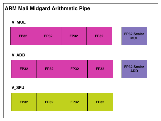
The above is a single Midgard arithmetic pipeline, in our example configured for FP32 operations. In it ARM uses a mix of both scalar and vector (SIMD) ALUs. Altogether ARM breaks it down as 3 vector ALUs and 2 scalar ALUs, each responsible for a specific type of operation.
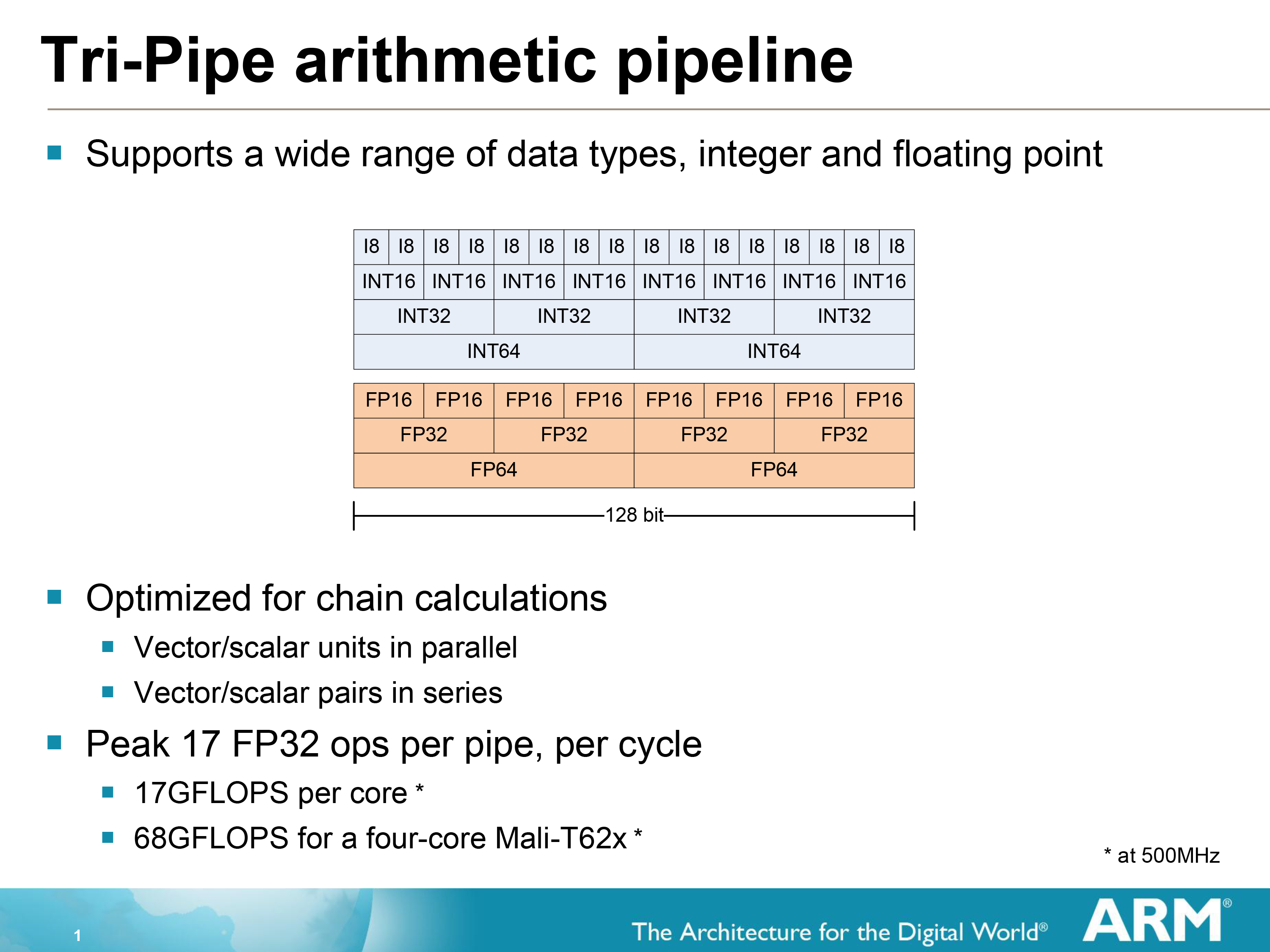
If we stop for a moment and look at the SIMD, we find out something very interesting about it as well. Remember earlier how we mentioned that Midgard is capable of 64bit operations? Well this is how they do it. Not with separate 64bit and 32bit units as in some other designs, but by using a single 128bit wide SIMD and decomposing operations based on their width. The 128bit SIMDs in a Midgard core can process 2 64 bit operations, 4 32bit operations, or even 8 16bit operations per clock cycle. Simply fill the SIMD with as many (identical) operations as will fit, and the SIMD will handle the rest.
The use of SIMDs and SIMD-like designs is not uncommon in GPUs, but it’s relatively rare to see a flexible SIMD of this nature. In the past other architecture designers have talked about this being a efficiency tradeoff – you lose some efficiency by using a flexible design rather than a rigid design – however in ARM’s case they have decided that they can meet all of their goals with a 128bit SIMD.
Jumping back up a level, from a hardware perspective a Midgard arithmetic pipeline is capable of up to 17 FP32 FLOPS. This is constructed as the following.
- 4 vector adds
- 4 vector multiplies
- 1 scalar add
- 1 scalar multiple
- 1 FDOT4 dot product (7 FLOPS)
The vector and scalar operations are relatively self-explanatory, while the dot products are a result of using the vector special functions unit. To that end every architecture possesses SFUs in some form to handle dot products, transcendentals, and other complex operations, but their inclusion in FLOPS counting is uncommon. Most architectures merely count FLOPS as adds and multiplies through the ubiquitous and all important MAD (Multiply-Add) instruction. NVIDIA’s forthcoming K1 (to pick a GPU with a desktop counterpart) has 192 FP32 ALUs, and via MADs can achieve up to 384 FLOPS per cycle.
Ultimately how ARM counts FLOPS is entirely up to them, but we do want to take a moment to rectify it with how we count FLOPS on our end. Dot products are a relatively common mathematical operation in rendering, enough so that it’s important to be able to do them quickly, but they are generally not counted for computing FLOPS.
Meanwhile for FP64 FLOPS, as one would expect Midgard’s performance is much lower. ARM does not provide the FLOPS breakdown for 64bit operations, but they tell us that it is a total of 5 FLOPS. Our best guess here is that 4 of those FLOPS are coming from the vector units (2 FP64 MADs) and then 1 more FP64 FLOP is coming off of the scalar units, which if our assumption is correct would imply that it is not capable of an FP64 MAD in 1 cycle. Overall on a MAD basis this puts FP64 performance at 5/10ths, or ½ FP32 performance, which is a very high FP64 performance ratio even compared to desktop GPU architectures.
Furthermore, in further rectifying how ARM presents some of its data with how we typically present data in our articles, we’re also going to be using a condensed version of the Midgard arithmetic pipeline from this point on. As most architectures either utilize ALUs that can perform a MAD on their own or simplify their descriptions to showcase 1 ALU (rather than explicitly over 2 ALUs as on Midgard), we will be using a condensed version of the Midgard arithmetic pipeline that is drawn in a similar manner. Since we always count a standard ALU as being capable of 2 FLOPs (SFUs withstanding), this makes our Midgard arithmetic pipeline illustration consistent with our previous illustrations. It’s for all intents and purposes the same pipeline, only condensed.
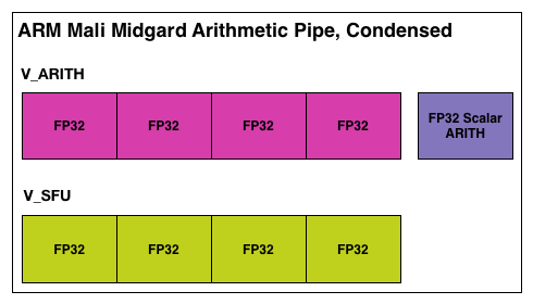
Finally, let’s take a quick look at a complete Midgard “tri pipe” core from an ALU standpoint. Since in T760 each core has 2 arithmetic units, a single core a just 2 of our condensed units. For a complete GPU this would then be multiplied by as many cores as the resulting design called for.


66 Comments
View All Comments
seanlumly - Thursday, July 3, 2014 - link
Given the "exotic" the ILP and the 128-bit VLIW SIMD, the Mali looks like an impressive performer. If a Mali T760MP10 is indeed a part fit for smartphone-level power consumption, then a quick linear-scaling -- given GFXBench scores of a T760MP4 -- would imply that such a GPU is very competitive with something like the adreno 420 and certainly impressive if scaled up further to a tablet-level power consumption. If, however, an MP10 consumes roughly as much as a K1 or GX6650, then I'm very sceptical about its competitive performance.I find the distribution of ALUs to memory units strange given mobile bandwidth limits. The Mali T760 in an 8-core configuration clocked at 600MHz will allow for 19.2 GB/s of load/store access (256-bits/clock: source ARM). This is quite high memory bandwidth, and an increase in GPU clocks or cores will likely yield idling load/stores units doing nothing but taking up valuable die area. Operations with high varying access, cache reads, and tile read/writes will of course make good use of these additional units, but it still seems like overkill on all but very memory-access heavy apps. ARM would know best, though I'm suspicious that so many load/store units are needed for common workloads. I would guess that in common scenarios, bandwidth to main memory would be exhausted long before all of the memory units were fully utilized on a Mali T760 of high core count (eg. MP12-16).
Decoupling the load/stores and texture units as their own "core" may allow more appropriate scaling to fit the bandwidth of the target system. A system with an ultra-high resolution, could be endowed with more load/stores and/or texture units. A system with a lower resolution could use less and opt for more ALUs in the same space. This would be similar to big.LITTLE (different cores for different targeted workloads). In this scenario, the memory unit cores could be scaled independently of the ALU cores, perfectly tailored to the target system.
EdvardS - Friday, July 4, 2014 - link
Remember that there is a cache system between those units and the SoC memory controller. Bandwidth to the cores is quite different from bandwidth to the DDR memory.seanlumly - Friday, July 4, 2014 - link
Indeed! Bandwidth to cache, tile memory, varying data, or textures would likely be more relevant with a tile-based renderer that often exploits spatial locality when processing batches of pixels. This is especially true with modern screen-space effects that do multiple dependent reads per display pixel (eg. SSAO), but are strongly confined to buffer fragments surrounding the target pixel. Such situations would value having many LS/Tex units at little penalty.But I do still like the idea of an independently scalable "memory" core (containing load/store/texure pipes) to complement a "math" core (containing ALUs). A high-performance system targeting a 720p display will likely consume far less bandwidth than one targeting a 4K display, and as such, it would be nice to trade LS/Tex units for more ALUs in such a case.
Such an arrangement may also enable ARM more leeway when making predictions about a new architecture -- no doubt the Midgard arch was in development many years before it saw implementation in a retail product, which means that ARM would have had to guess trends (eg. resolution) far in advance to attain the right balance of on-chip units per core; independently scalable memory-cores would be more forgiving if the trends turned out not match the initial predictions.
seanlumly - Friday, July 4, 2014 - link
Actually, I am starting to understand the motivation behind the ratio of ALUs to Memory units in a Midgard core. I notice in GFXBench 3.0 "Manhattan", that the Mali T760MP4 (Rockchip rk3288) performs incredibly well at 720p, but it's performance drops off more than proportionately as the resolution increases. This may imply that in these higher than 720p scenarios, the 4-core variant of GPU may not be able to keep up with the memory demands, as computation should scale very close to proportionally.Thus the 1080p offscreen score for the Mail T760 MP4 in the GFXBench 3.0 (offline) database may be misleading as the MP4 may be a bit small for this resolution, and thus the performance may be low relative to its competition. A T760 MP8 would likely more than double the performance for a doubling of the resolution, pushing something like the Mali T760 MP8 well beyond the competition, at what I suspect are similar levels of power and die-size. I predict that a T760 MP8 would get slightly north of 16fps in GFXBench 3.0 (assuming adequate bandwidth to DDR). Even an MP6 variant of the GPU (as was the case with the T628 MP6 in the Exynos 5420) should put it more-or-less on-par with the competition!
The Mali performs even better in the GFXBench 2.7 "T-Rex" test, where a small 4-core Mali T760 MP4 surpasses the competition at 720p and even sub-720p resolutions in some instances! This is incredible. In this case, it seems that the test is more computation bound, as there is a more proportional scaling between performance and resolution.
I hope that future GPUs consider using the T760 in higher-core-count configurations. I still like the idea of a Memory-core, though I have little doubt that a Mali GPU of evenly matched size can go toe-to-toe with the competition.
Frenetic Pony - Friday, July 4, 2014 - link
Every time I read an overview of a SoC GPU I am so, so glad I don't do anything with mobile stuff. "We support tessellation! I mean, don't actually do it. Ever. But you know, it's supported."kkb - Friday, July 4, 2014 - link
How come there is no comparison with intel GPUs like the ones in Baytrail?darkich - Friday, July 4, 2014 - link
Because there is no comparison phrase.That GPU is completely inferior compared to latest Mali, PowerVR and Adreno architectures
Krysto - Friday, July 4, 2014 - link
Word.kkb - Monday, July 7, 2014 - link
well.. I don't really agree. Please look at the AT review from last week or so.. http://www.anandtech.com/show/8197/samsung-galaxy-...MEMO pad is a baytrail product and definitely performs better than MALI devices.
darkich - Monday, July 7, 2014 - link
Get your facts and reading skills in order.Firstly, the GPU in Memo Pad is definitely not definitely performing better than even the Mali T628, in fact those very tests show it trades blows with it, mostly due to much lower resolution screen.
Secondly, do you realize that the T760 is MUCH faster than T628?
You can see here that it is basically comparable to the Tegra K1 and even the intimidating Series 6XT doesn't trounce it.
Rest assured that any of these three, as well as the Adreno 420, is way above the ULP HD graphics chip