ARM’s Mali Midgard Architecture Explored
by Ryan Smith on July 3, 2014 11:00 AM ESTMidgard’s Execution Model: ILP, not TLP
Having seen the makeup of a Midgard arithmetic unit, we can finally get to the subject of thread execution on Midgard, and in the process get to what’s easily the least traditional aspect of the Midgard GPU.
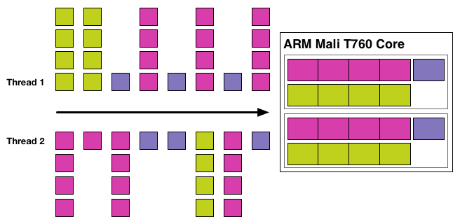
As we mentioned before, Midgard is based on the idea of using VLIW with SIMDs, or as ARM likes to call it Sequential Long Instruction Word. In this execution model the Midgard shader compiler attempts to construct a single word of instructions in order to fill as many of the ALUs in an arithmetic pipeline as is possible. As is common for VLIW designs, this requires extracting a degree of Instruction Level Parallelism from the instructions being fed to the shader compiler, both to find operations that can be placed together on the SIMD units and to find operations that can then fill any of the otherwise idle units in a Midgard arithmetic pipeline. There is no superscalar execution going on here, but to make full use of a Midgard arithmetic unit you need to be able to bundle several operations together into the single VLIW word.
Depending on who you ask, an ILP-centric design either makes a great deal of sense or is difficult to program for, depending of course on the specific quirks of an architecture. From a hardware perspective this is very simple because the compiler does all the work while the hardware itself is merely executing VLIW instructions as requested. The hardware is not doing any scheduling or hazard checking on its own, and only really needs to deal with a stall (when a memory operand isn’t available in time). This saves die space and this saves power, and because all of your instructions in an arithmetic unit are from the same thread then you can save even more space because you have a group of ALUs working on the same thread with its data elements adjacent to each other.
Of all of the SoC_class GPUs we’ve looked at that are currently paired with ARM processors – NVIDIA’s Kepler and Imagination’s Rogue – both are designs that rely at least in part on ILP. Both also happen to be superscalar (something that’s not the case for Midgard), but at a basic level Midgard is in good company with its ILP-centric design.
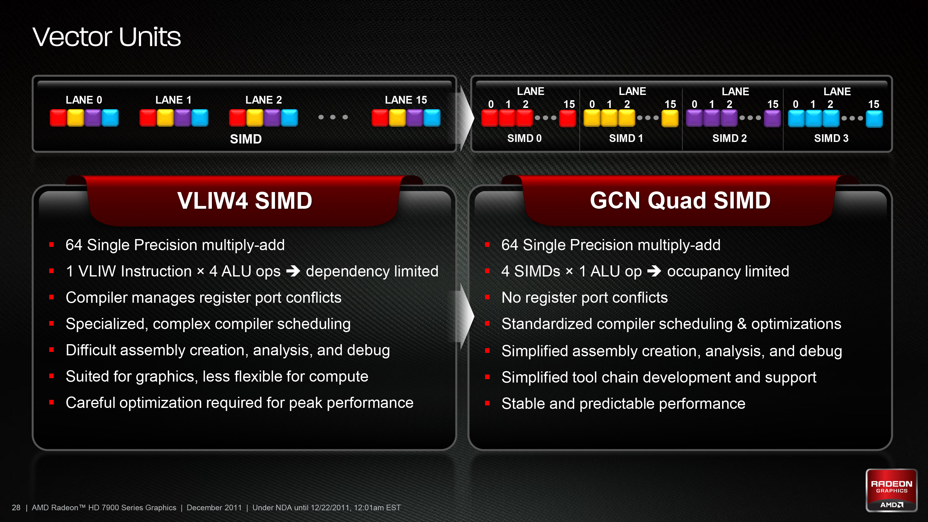
On the other hand we have seen one other company attempt a VLIW and ILP-centric design in recent history only to abandon it. AMD used a vaguely similar VLIW design for their Radeon HD 2000 through HD 6000 parts, only to abandon VLIW for a non-VLIW design in 2011. At the time they cited that compute workloads weren’t mapping well to their design, and even graphics workloads were increasingly becoming less optimal. AMD’s replacement architecture, Graphics Core Next, used no ILP and relied entirely on Thread Level Parallelism.
A Summary of AMD's Experiences With VLIW versus TLP SIMD
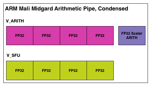
Ultimately the intended use case for Midgard is first and foremost graphics, and this is something that by all accounts it seems to do well at. For a simpler GPU design such as what would be suitable for an SoC-class GPU, VLIW is still a strong fit in ARM’s case because the 128bit vector SIMD maps well to RGBA shader operations (one color channel per SIMD lane) while the scalar unit covers anything else that doesn’t map well to the vector units. To that end we won’t spend too much more time covering the pros and cons of an ILP-centric VLIW design, but we did want to cover the history and how it compares to some other architectures.
Meanwhile, for anyone curious about the pipeline in an individual Midgard ALU, ARM also opened up to us on that front. In a very rare occasion in the GPU world ARM told us how deep their pipeline is, coming in at up to 128 stages deep for the entire Midgard pipeline. The artihmetic pipeline itself is under 30 stages deep but each pipeline of the tri-pipe design is a different length. Since we don’t know the depth of any other GPU pipelines we don’t have anything of substance to compare it to, but it is notable that ARM’s execution model is consistent with GPU execution models in general. A 128 stage deep pipeline invokes a high latency, high throughput machine that is interleaving a large number of threads to keep the pipeline full, which is in a nutshell an accurate description for GPUs in general. In any case, for Midgard ARM provides a further twist by bypassing misses (a failed attempt to read or write a piece of data) entirely; misses result in an instruction restart, rather than stalling the pipeline and all of the threads in it while waiting for the miss to be resolved.
Looking at the larger picture then, now that we how a single thread executes across one Midgard arithmetic unit let’s see how multiple arithmetic units work in concert. Or rather let’s not, because they don’t.
In the larger picture Midgard deviates from any other modern GPU we’ve seen in a very important way: Midgard does not extract thread level parallelism.
Every other GPU, be it Imagination, NVIDIA, AMD, or Intel, and whether it relies on ILP or not, also relies on thread level parallelism (TLP) to organize their work. In these designs multiple threads are bundled together and sent through an array of ALUs at once, where each thread in turn represents what is essentially a single pixel. Due to their spatial locality these pixels-as-threads are run together, the idea being that due to their locality they’re almost certainly going to have the same instruction applied, and in the end can be sent through ALUs that operate as a group and not independently. These wavefronts are a basic tenet of modern GPUs, whether it’s groups of 16 threads per cycle as is the case for AMD and Imagination, or groups of 32 threads per cycle as is the case for NVIDIA.
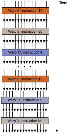
An Example of Wavefront/Warp Thread Execution On Other Architectures
But it’s this basic tenet that the Mali team has wanted to challenge, and in doing so they have put together an architecture in Midgard (and Utgard before it) that extracts no TLP from threads and executes each and every one of them independently. This, more than anything else, is the element that sets Midgard’s design apart from anything else we’ve seen so far.
As a result of this design decision, each arithmetic pipeline in Midgard is essentially its own CPU, consuming threads and processing them independently. Even in a single Mail-T760 tri pipe where there are 2 arithmetic units in a block these arithmetic units act on their own, working separately from one-another. Or to put this in to practice, in a large Midgard configuration such as T760MP16, this would mean a full 32 threads (16 cores * 2 math units) are being actively and independently executed.
Taken at face value then, this is a design that is very unorthodox and comes with a significant number of pitfalls that thread level parallelism is designed to compensate for. On the whole TLP is considered to be very easy to extract due to the spatial locality of pixels, which is all the more reason why on the desktop AMD went from a design that mixed ILP and TLP to a design that only utilized TLP. Furthermore because of the locality of pixels and threads, the ALUs in a design that does utilize TLP – typically a 16 or 32 wide array of SIMD ALUs – could be smaller due to the fact that they did not need the means to act independently, allowing more ALUs to be placed on such a GPU than would otherwise be possible.
But on the other hand TLP-centric designs do have their own drawbacks, and these are the reasons that ARM believes their non-TLP Midgard architecture is the way to go. First and foremost, TLP designs can only excel when threads/pixels need to flow together. If they need to go their separate ways, say due to a branching operation, then execution is slowed down to handle that branch. Alternatively, a group of threads that are branching may not be large enough to fill all 16/32 slots in a wavefront, in which case there are ALUs in the array executing the wavefront are going unused.

Midgard in contrast does not suffer from any thread related occupancy issues beyond very light workloads where even 32 threads (T760MP16) cannot be found, in which case Midgard gets to shut off whole cores. In fact because of this Midgard gets to branch for next to free due to the fact that there aren’t any other threads an arithmetic pipeline must concern itself with. Midgard arithmetic units can branch as they please and access memory as they please, an especially convenient scenario since tiling is already bounding the work area. At the same time however, this means that Midgard is going to be at its best in code with lots of branches, as otherwise in code with minimal branching will map well to traditional TLP-centric designs.
Meanwhile on the matter of tiling, this brings up another point ARM likes to make about Midgard versus TLP-centric designs, which is that they believe that wavefronts and tile based renderers are poorly matched. At times the limited number of threads/pixels in tiles would certainly exacerbate any issues keeping wavefronts filled with threads, among other things.
With that said from a theoretical perspective there’s not much more we can say on the matter other than to cover the execution model and the potential strengths and weaknesses of it. Other than that the proof is in the pudding, and that how well ARM’s unorthodox architecture performs is ultimately what determines if ARM has made the best move in creating such a unique architecture, or if there is a reason everyone else invests in thread level parallelism.
But for what it is worth, this design does go back to Utgard, and Utgard was (and continues to be) a solid performer for ARM. It has sold well over the years and would strongly suggest that a TLP insensitive architecture can in fact map well to workloads, at least for OpenGL ES 2.0 graphics.


66 Comments
View All Comments
3DPowerFX - Thursday, July 3, 2014 - link
Once again, AnandTech has published a great article! Thanks ARM and AnandTech.Just one point. there is a small mistake in the article about Samsung Exynos 3470 GPU. It's not Mali 450MP but the undead Mali 400MP GPU. Although it would be nice to have the latest one.
Cogman - Thursday, July 3, 2014 - link
On transaction elimination. A movie is actually much worse about being eliminated than anything else. The only saving grace for a movie is the fact that the FPS are often much lower than what the device is natively putting out (so 60fps is a typical display refresh rate whereas movies typically operate at 24->30fps). After that, everything changes right down to the smallest detail. This is the grainy effect that you see in movies.For games, there could be some benefit assuming the game isn't a high action one. The biggest win will be still images (90% of what these displays are going to be displaying).
EdvardS - Thursday, July 3, 2014 - link
Movies are not actually that bad. Remember that videos we watch on our devices have already been compressed with lossy algorithms looking for temporal resemblance, which seems to boost the transaction elimination efficiency as well.BMNify - Thursday, July 3, 2014 - link
gem did a writup , but i cant find it now !, but take a look here as regards transaction elimination http://community.arm.com/groups/arm-mali-graphics/...BTW "the grainy effect that you see in movies" have absolutely nothing to do with frame rate
its put there (as in artificially) by the post processing due to the fact today everyone's using 8bit per pixel as in Rec. 709 (HDTV) color space that produces banding and other visible anomalies not the new official Rec. 2020 (UHDTV/UHD-1/UHD-2) real 10bit/12bit color space we will see soon.
tuxRoller - Thursday, July 3, 2014 - link
Consider asking red hat's rob clark. He's been reverse engineering the adreno arch (his driver, freedreno (https://github.com/freedreno/freedreno/wiki) however, is not a reverse engineered adreno driver) for a few years now and can almost certainly give you at least that much info.His blog is at http://bloggingthemonkey.blogspot.com, and he's a super nice guy.
jwcalla - Friday, July 4, 2014 - link
Qualcomm is a really closed company. They just did a massive DCMA takedown on GitHub: https://github.com/github/dmca/blob/master/2014-07...Their software side isn't that great either.
tuxRoller - Friday, July 4, 2014 - link
I'm not sure why this is addressed to me. Although I expect AT will ignore what I've written so as not to upset their corporate friends, what I suggested is what they should do if they are really interested in the tech.What's strange to me is that they did something similar with their analysis of Cyclone to what I'm suggesting they do, except in the Qualcomm case the work is done by someone else.
Death666Angel - Thursday, July 3, 2014 - link
Awesome to see this here! I hope the Adreno team will follow suite soon and lay their doubts to rest."LG’s Viewty" Holy shit, that way my 2nd ever phone (after my first flip phone got broken when I rammed a car with my bike). That thing was pretty bad all in all. But the slow motion camera was great for its time! :D It broke too while I was in a fight, but that was the last one. Touch Pro 2, Galaxy S2, Galaxy Nexus and LG G2 all working fine till this day. :D
Willardjuice - Thursday, July 3, 2014 - link
"From a sales perspective this means ARM can offer the CPU and GPU designs together in a bundle, but perhaps more importantly it means they have the capability design the two in concert with each other, being in the position of the sole creator of the ARM ISA."lol, the bundle aspect is far more important for ARM gpu sales. ;)
skiboysteve - Thursday, July 3, 2014 - link
Truth. Basically makes it so a competitor needs to show a significant performance, power, feature, or cost difference before it's worth an integrator investing in breaking apart the bundle