ARM’s Mali Midgard Architecture Explored
by Ryan Smith on July 3, 2014 11:00 AM ESTMidgard’s Arithmetic Pipelines
Having taken a look at Midgard’s architecture from a high level perspective, we next want to dive deep into the heart of Midgard: its arithmetic pipelines. This is where the bulk of the work takes place on any modern GPU, and in most cases real-world GPU performance significantly hinges on the design decisions made here. Furthermore this is where Midgard’s most unconventional design decisions lie, and as a result it’s the arithmetic pipelines that make Midgard stand apart from anything else we’ve seen.
ARM describes Midgard as a Very Long Instruction Word (VLIW) design with Single Instruction Multiple Data (SIMD) characteristics (though officially it is called Sequential Long Instruction Word). What this means is that at a high level ARM is feeding multiple ALUs, including SIMD units, with a single long word of instructions. But perhaps it’s better we start at a low level instead.
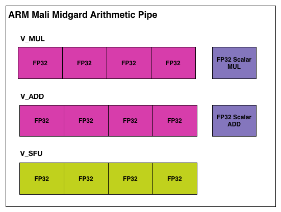
The above is a single Midgard arithmetic pipeline, in our example configured for FP32 operations. In it ARM uses a mix of both scalar and vector (SIMD) ALUs. Altogether ARM breaks it down as 3 vector ALUs and 2 scalar ALUs, each responsible for a specific type of operation.
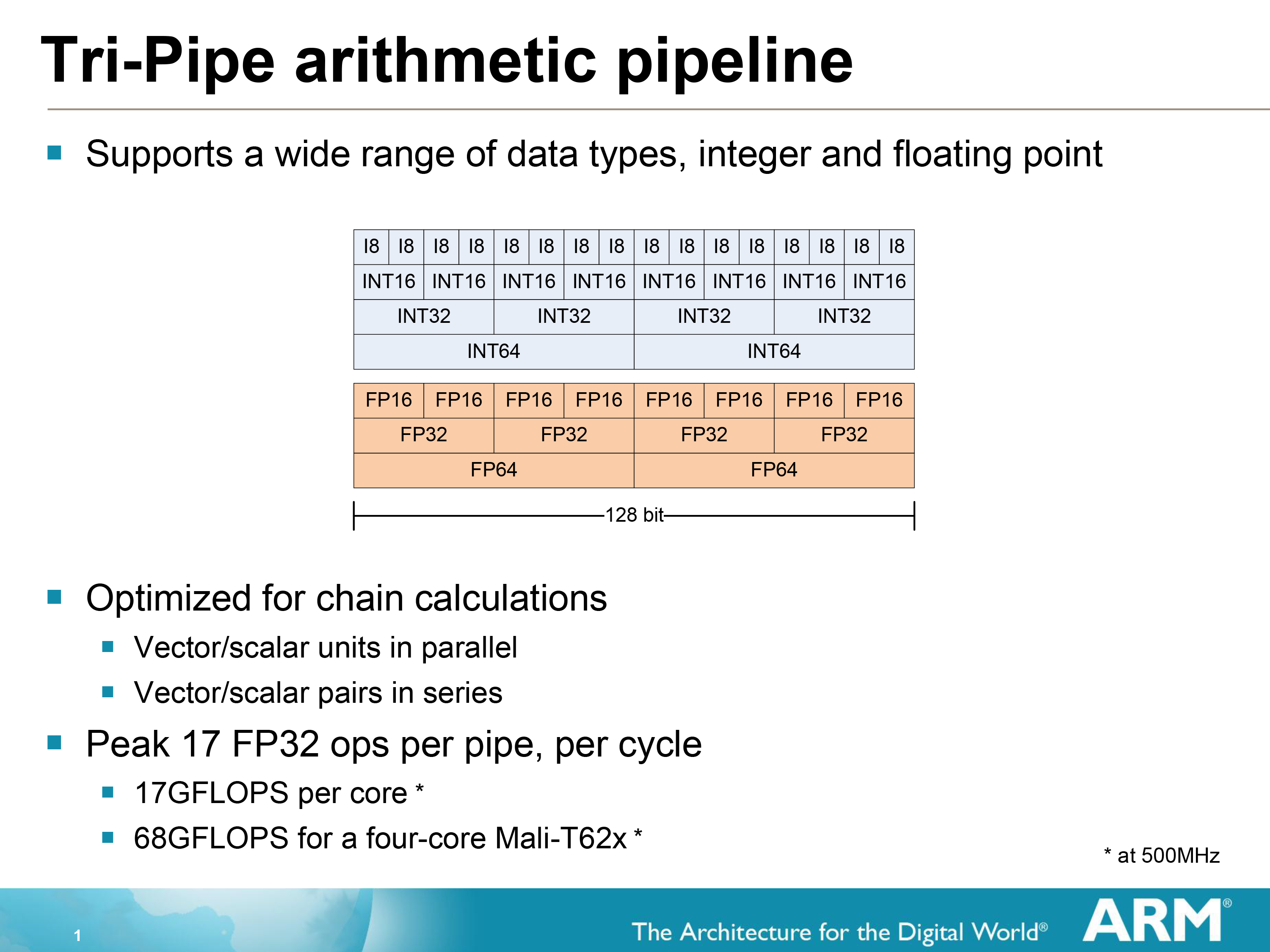
If we stop for a moment and look at the SIMD, we find out something very interesting about it as well. Remember earlier how we mentioned that Midgard is capable of 64bit operations? Well this is how they do it. Not with separate 64bit and 32bit units as in some other designs, but by using a single 128bit wide SIMD and decomposing operations based on their width. The 128bit SIMDs in a Midgard core can process 2 64 bit operations, 4 32bit operations, or even 8 16bit operations per clock cycle. Simply fill the SIMD with as many (identical) operations as will fit, and the SIMD will handle the rest.
The use of SIMDs and SIMD-like designs is not uncommon in GPUs, but it’s relatively rare to see a flexible SIMD of this nature. In the past other architecture designers have talked about this being a efficiency tradeoff – you lose some efficiency by using a flexible design rather than a rigid design – however in ARM’s case they have decided that they can meet all of their goals with a 128bit SIMD.
Jumping back up a level, from a hardware perspective a Midgard arithmetic pipeline is capable of up to 17 FP32 FLOPS. This is constructed as the following.
- 4 vector adds
- 4 vector multiplies
- 1 scalar add
- 1 scalar multiple
- 1 FDOT4 dot product (7 FLOPS)
The vector and scalar operations are relatively self-explanatory, while the dot products are a result of using the vector special functions unit. To that end every architecture possesses SFUs in some form to handle dot products, transcendentals, and other complex operations, but their inclusion in FLOPS counting is uncommon. Most architectures merely count FLOPS as adds and multiplies through the ubiquitous and all important MAD (Multiply-Add) instruction. NVIDIA’s forthcoming K1 (to pick a GPU with a desktop counterpart) has 192 FP32 ALUs, and via MADs can achieve up to 384 FLOPS per cycle.
Ultimately how ARM counts FLOPS is entirely up to them, but we do want to take a moment to rectify it with how we count FLOPS on our end. Dot products are a relatively common mathematical operation in rendering, enough so that it’s important to be able to do them quickly, but they are generally not counted for computing FLOPS.
Meanwhile for FP64 FLOPS, as one would expect Midgard’s performance is much lower. ARM does not provide the FLOPS breakdown for 64bit operations, but they tell us that it is a total of 5 FLOPS. Our best guess here is that 4 of those FLOPS are coming from the vector units (2 FP64 MADs) and then 1 more FP64 FLOP is coming off of the scalar units, which if our assumption is correct would imply that it is not capable of an FP64 MAD in 1 cycle. Overall on a MAD basis this puts FP64 performance at 5/10ths, or ½ FP32 performance, which is a very high FP64 performance ratio even compared to desktop GPU architectures.
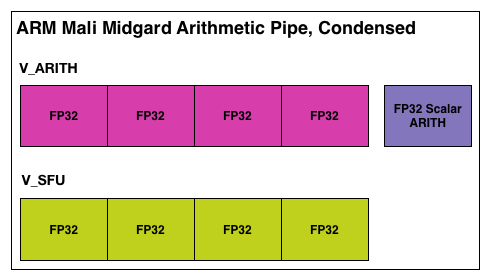
Furthermore, in further rectifying how ARM presents some of its data with how we typically present data in our articles, we’re also going to be using a condensed version of the Midgard arithmetic pipeline from this point on. As most architectures either utilize ALUs that can perform a MAD on their own or simplify their descriptions to showcase 1 ALU (rather than explicitly over 2 ALUs as on Midgard), we will be using a condensed version of the Midgard arithmetic pipeline that is drawn in a similar manner. Since we always count a standard ALU as being capable of 2 FLOPs (SFUs withstanding), this makes our Midgard arithmetic pipeline illustration consistent with our previous illustrations. It’s for all intents and purposes the same pipeline, only condensed.
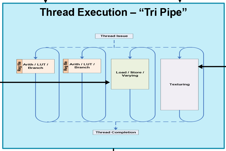
Finally, let’s take a quick look at a complete Midgard “tri pipe” core from an ALU standpoint. Since in T760 each core has 2 arithmetic units, a single core a just 2 of our condensed units. For a complete GPU this would then be multiplied by as many cores as the resulting design called for.


66 Comments
View All Comments
3DPowerFX - Thursday, July 3, 2014 - link
Once again, AnandTech has published a great article! Thanks ARM and AnandTech.Just one point. there is a small mistake in the article about Samsung Exynos 3470 GPU. It's not Mali 450MP but the undead Mali 400MP GPU. Although it would be nice to have the latest one.
Cogman - Thursday, July 3, 2014 - link
On transaction elimination. A movie is actually much worse about being eliminated than anything else. The only saving grace for a movie is the fact that the FPS are often much lower than what the device is natively putting out (so 60fps is a typical display refresh rate whereas movies typically operate at 24->30fps). After that, everything changes right down to the smallest detail. This is the grainy effect that you see in movies.For games, there could be some benefit assuming the game isn't a high action one. The biggest win will be still images (90% of what these displays are going to be displaying).
EdvardS - Thursday, July 3, 2014 - link
Movies are not actually that bad. Remember that videos we watch on our devices have already been compressed with lossy algorithms looking for temporal resemblance, which seems to boost the transaction elimination efficiency as well.BMNify - Thursday, July 3, 2014 - link
gem did a writup , but i cant find it now !, but take a look here as regards transaction elimination http://community.arm.com/groups/arm-mali-graphics/...BTW "the grainy effect that you see in movies" have absolutely nothing to do with frame rate
its put there (as in artificially) by the post processing due to the fact today everyone's using 8bit per pixel as in Rec. 709 (HDTV) color space that produces banding and other visible anomalies not the new official Rec. 2020 (UHDTV/UHD-1/UHD-2) real 10bit/12bit color space we will see soon.
tuxRoller - Thursday, July 3, 2014 - link
Consider asking red hat's rob clark. He's been reverse engineering the adreno arch (his driver, freedreno (https://github.com/freedreno/freedreno/wiki) however, is not a reverse engineered adreno driver) for a few years now and can almost certainly give you at least that much info.His blog is at http://bloggingthemonkey.blogspot.com, and he's a super nice guy.
jwcalla - Friday, July 4, 2014 - link
Qualcomm is a really closed company. They just did a massive DCMA takedown on GitHub: https://github.com/github/dmca/blob/master/2014-07...Their software side isn't that great either.
tuxRoller - Friday, July 4, 2014 - link
I'm not sure why this is addressed to me. Although I expect AT will ignore what I've written so as not to upset their corporate friends, what I suggested is what they should do if they are really interested in the tech.What's strange to me is that they did something similar with their analysis of Cyclone to what I'm suggesting they do, except in the Qualcomm case the work is done by someone else.
Death666Angel - Thursday, July 3, 2014 - link
Awesome to see this here! I hope the Adreno team will follow suite soon and lay their doubts to rest."LG’s Viewty" Holy shit, that way my 2nd ever phone (after my first flip phone got broken when I rammed a car with my bike). That thing was pretty bad all in all. But the slow motion camera was great for its time! :D It broke too while I was in a fight, but that was the last one. Touch Pro 2, Galaxy S2, Galaxy Nexus and LG G2 all working fine till this day. :D
Willardjuice - Thursday, July 3, 2014 - link
"From a sales perspective this means ARM can offer the CPU and GPU designs together in a bundle, but perhaps more importantly it means they have the capability design the two in concert with each other, being in the position of the sole creator of the ARM ISA."lol, the bundle aspect is far more important for ARM gpu sales. ;)
skiboysteve - Thursday, July 3, 2014 - link
Truth. Basically makes it so a competitor needs to show a significant performance, power, feature, or cost difference before it's worth an integrator investing in breaking apart the bundle