ARM’s Mali Midgard Architecture Explored
by Ryan Smith on July 3, 2014 11:00 AM ESTMidgard’s Execution Model: ILP, not TLP
Having seen the makeup of a Midgard arithmetic unit, we can finally get to the subject of thread execution on Midgard, and in the process get to what’s easily the least traditional aspect of the Midgard GPU.
As we mentioned before, Midgard is based on the idea of using VLIW with SIMDs, or as ARM likes to call it Sequential Long Instruction Word. In this execution model the Midgard shader compiler attempts to construct a single word of instructions in order to fill as many of the ALUs in an arithmetic pipeline as is possible. As is common for VLIW designs, this requires extracting a degree of Instruction Level Parallelism from the instructions being fed to the shader compiler, both to find operations that can be placed together on the SIMD units and to find operations that can then fill any of the otherwise idle units in a Midgard arithmetic pipeline. There is no superscalar execution going on here, but to make full use of a Midgard arithmetic unit you need to be able to bundle several operations together into the single VLIW word.
Depending on who you ask, an ILP-centric design either makes a great deal of sense or is difficult to program for, depending of course on the specific quirks of an architecture. From a hardware perspective this is very simple because the compiler does all the work while the hardware itself is merely executing VLIW instructions as requested. The hardware is not doing any scheduling or hazard checking on its own, and only really needs to deal with a stall (when a memory operand isn’t available in time). This saves die space and this saves power, and because all of your instructions in an arithmetic unit are from the same thread then you can save even more space because you have a group of ALUs working on the same thread with its data elements adjacent to each other.
Of all of the SoC_class GPUs we’ve looked at that are currently paired with ARM processors – NVIDIA’s Kepler and Imagination’s Rogue – both are designs that rely at least in part on ILP. Both also happen to be superscalar (something that’s not the case for Midgard), but at a basic level Midgard is in good company with its ILP-centric design.
On the other hand we have seen one other company attempt a VLIW and ILP-centric design in recent history only to abandon it. AMD used a vaguely similar VLIW design for their Radeon HD 2000 through HD 6000 parts, only to abandon VLIW for a non-VLIW design in 2011. At the time they cited that compute workloads weren’t mapping well to their design, and even graphics workloads were increasingly becoming less optimal. AMD’s replacement architecture, Graphics Core Next, used no ILP and relied entirely on Thread Level Parallelism.
A Summary of AMD's Experiences With VLIW versus TLP SIMD
Ultimately the intended use case for Midgard is first and foremost graphics, and this is something that by all accounts it seems to do well at. For a simpler GPU design such as what would be suitable for an SoC-class GPU, VLIW is still a strong fit in ARM’s case because the 128bit vector SIMD maps well to RGBA shader operations (one color channel per SIMD lane) while the scalar unit covers anything else that doesn’t map well to the vector units. To that end we won’t spend too much more time covering the pros and cons of an ILP-centric VLIW design, but we did want to cover the history and how it compares to some other architectures.
Meanwhile, for anyone curious about the pipeline in an individual Midgard ALU, ARM also opened up to us on that front. In a very rare occasion in the GPU world ARM told us how deep their pipeline is, coming in at up to 128 stages deep for the entire Midgard pipeline. The artihmetic pipeline itself is under 30 stages deep but each pipeline of the tri-pipe design is a different length. Since we don’t know the depth of any other GPU pipelines we don’t have anything of substance to compare it to, but it is notable that ARM’s execution model is consistent with GPU execution models in general. A 128 stage deep pipeline invokes a high latency, high throughput machine that is interleaving a large number of threads to keep the pipeline full, which is in a nutshell an accurate description for GPUs in general. In any case, for Midgard ARM provides a further twist by bypassing misses (a failed attempt to read or write a piece of data) entirely; misses result in an instruction restart, rather than stalling the pipeline and all of the threads in it while waiting for the miss to be resolved.
Looking at the larger picture then, now that we how a single thread executes across one Midgard arithmetic unit let’s see how multiple arithmetic units work in concert. Or rather let’s not, because they don’t.
In the larger picture Midgard deviates from any other modern GPU we’ve seen in a very important way: Midgard does not extract thread level parallelism.
Every other GPU, be it Imagination, NVIDIA, AMD, or Intel, and whether it relies on ILP or not, also relies on thread level parallelism (TLP) to organize their work. In these designs multiple threads are bundled together and sent through an array of ALUs at once, where each thread in turn represents what is essentially a single pixel. Due to their spatial locality these pixels-as-threads are run together, the idea being that due to their locality they’re almost certainly going to have the same instruction applied, and in the end can be sent through ALUs that operate as a group and not independently. These wavefronts are a basic tenet of modern GPUs, whether it’s groups of 16 threads per cycle as is the case for AMD and Imagination, or groups of 32 threads per cycle as is the case for NVIDIA.
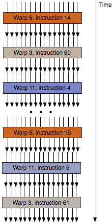
An Example of Wavefront/Warp Thread Execution On Other Architectures
But it’s this basic tenet that the Mali team has wanted to challenge, and in doing so they have put together an architecture in Midgard (and Utgard before it) that extracts no TLP from threads and executes each and every one of them independently. This, more than anything else, is the element that sets Midgard’s design apart from anything else we’ve seen so far.
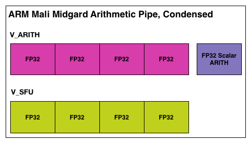
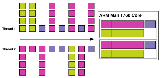
As a result of this design decision, each arithmetic pipeline in Midgard is essentially its own CPU, consuming threads and processing them independently. Even in a single Mail-T760 tri pipe where there are 2 arithmetic units in a block these arithmetic units act on their own, working separately from one-another. Or to put this in to practice, in a large Midgard configuration such as T760MP16, this would mean a full 32 threads (16 cores * 2 math units) are being actively and independently executed.
Taken at face value then, this is a design that is very unorthodox and comes with a significant number of pitfalls that thread level parallelism is designed to compensate for. On the whole TLP is considered to be very easy to extract due to the spatial locality of pixels, which is all the more reason why on the desktop AMD went from a design that mixed ILP and TLP to a design that only utilized TLP. Furthermore because of the locality of pixels and threads, the ALUs in a design that does utilize TLP – typically a 16 or 32 wide array of SIMD ALUs – could be smaller due to the fact that they did not need the means to act independently, allowing more ALUs to be placed on such a GPU than would otherwise be possible.
But on the other hand TLP-centric designs do have their own drawbacks, and these are the reasons that ARM believes their non-TLP Midgard architecture is the way to go. First and foremost, TLP designs can only excel when threads/pixels need to flow together. If they need to go their separate ways, say due to a branching operation, then execution is slowed down to handle that branch. Alternatively, a group of threads that are branching may not be large enough to fill all 16/32 slots in a wavefront, in which case there are ALUs in the array executing the wavefront are going unused.

Midgard in contrast does not suffer from any thread related occupancy issues beyond very light workloads where even 32 threads (T760MP16) cannot be found, in which case Midgard gets to shut off whole cores. In fact because of this Midgard gets to branch for next to free due to the fact that there aren’t any other threads an arithmetic pipeline must concern itself with. Midgard arithmetic units can branch as they please and access memory as they please, an especially convenient scenario since tiling is already bounding the work area. At the same time however, this means that Midgard is going to be at its best in code with lots of branches, as otherwise in code with minimal branching will map well to traditional TLP-centric designs.
Meanwhile on the matter of tiling, this brings up another point ARM likes to make about Midgard versus TLP-centric designs, which is that they believe that wavefronts and tile based renderers are poorly matched. At times the limited number of threads/pixels in tiles would certainly exacerbate any issues keeping wavefronts filled with threads, among other things.
With that said from a theoretical perspective there’s not much more we can say on the matter other than to cover the execution model and the potential strengths and weaknesses of it. Other than that the proof is in the pudding, and that how well ARM’s unorthodox architecture performs is ultimately what determines if ARM has made the best move in creating such a unique architecture, or if there is a reason everyone else invests in thread level parallelism.
But for what it is worth, this design does go back to Utgard, and Utgard was (and continues to be) a solid performer for ARM. It has sold well over the years and would strongly suggest that a TLP insensitive architecture can in fact map well to workloads, at least for OpenGL ES 2.0 graphics.


66 Comments
View All Comments
darkich - Friday, July 4, 2014 - link
You guys are missing the fact that Snapdragon 805 can reach a much higher memory bandwidth than Tegra K1.TheJian - Saturday, July 5, 2014 - link
But it still loses to K1 in most gpu stuff (all?). You're forgetting AMD/NV have had 20yrs of trying to figure out how to get the most they can from bandwidth for gaming. The devs have had that long working with their hardware also (game devs I mean). Everyone else has to play catch up here for years as they've never had to do anything game wise until last year or so as android etc gaming pumped up a bit.That is why you see ZERO Qcom optimized games (or did I miss one?) :) It's easier to optimize for a chip you already know inside out (amd/nv). I even went to Qcom's gaming page just to see if there were any games they had on their list that were REQUIRING snapdragon to see xx effects etc. There were none last I checked. All the games are just on googleplay with no snapdragon mention (like on NV games they say THD, and these games look quite a bit better than the regular versions) as they appear to work on ALL players chips. Google seems to be realizing K1 is where you want to be on gpu's at least for gaming centric stuff/automotive and I'd expect devs to continue to favor NV for optimizations as they don't need to learn a thing about k1 it's KEPLER which they've already spent 2yrs+ playing with (probably longer as they get dev versions long before we get a retail card so games can be made/optimized for them by the time they hit).
At 20nm xbox360/ps3 will be left behind as new games keep getting made on mobile. If you're not on xbox1/ps4 you'll be buying some cheap 20nm console box that has cheap games ($2-20 vs. $60 for xbox1/ps4) and as good or better graphics than last gen xbox360/ps3. GDC 2013 & 2014 surveys show devs are already massively making games for mobile and as 20nm kicks in everyone has K1 power levels or more. These android consoles/tv's etc will have more tricks than those ancient consoles so you should be able to get much better gaming experience on them for $100-200. The games pricing alone is a draw for poor people. With the ports happening right an left now of quality PC/console games and super cheap pricing there is even more reason to run to mobile for poor people who never played them before (half-life2, trine2, Serious Sam3BFE, none sold more than 11mil or so). There are a billion android users and most clearly have played none of this stuff even the console ports like Final Fantasy games, GTA games etc (on or off PC also doesn't matter) haven't been played by more than 10mil or so combined each. Lost of great stuff for poor people to pick up for under $10 in ports until the REAL new games for mobile hit this xmas/next xmas. All of the stuff the dev surveys show they've been working on will hit this year or next, and they are not angry birds games.
przemo_li - Tuesday, July 8, 2014 - link
Alternative view on Google stance:Nvidia is just first vendor that allowed them to show more features than are possible on Apples A7.
(Mobile-only vendors are not interested in full OpenGL...)
TheJian - Sunday, July 6, 2014 - link
If they're worried about lawsuits (odd they'd say that without merit), they must have had their lawyers tell them they'd be sued due to stealing tech that is probably from AMD/NV. DMCA takedowns, completely closing the kimono so to speak shows they are afraid for good reason. It isn't just competitor crap as nobody else is afraid of that it seems. The same tricks are being used by almost everyone to a large degree. So it seems to me they clearly owe someone some money and don't want to pay. They will probably show their details once they remove that stuff from a future gen soc or never I guess if they just can't remove it for some reason :)mczak - Thursday, July 3, 2014 - link
You could add Intel HD graphics (baytrail) though. Also quite interesting architecture-wise imho.btw some small correction wavefront size for amd (gcn) is 64, not 16 (I think this was wrong on older anandtech articles too). The simd size is 16 indeed but the same instruction is executed for 4 clocks always (on 16 different elements of the wavefront each clock).
mczak - Thursday, July 3, 2014 - link
Here's actually an explanation how the wavefront size of 64 works for gcn:http://devgurus.amd.com/thread/168154
Achtung_BG - Thursday, July 3, 2014 - link
My first touch phone is black LG Viewty in 2008 with Mali GPU :) :) :) If you have new article for android extention pack comparison with full Open GL will be very intrasting.Jedibeeftrix - Thursday, July 3, 2014 - link
yes please.i'd like to know:
1. how long until the AEP is rolled back into what will be OpenGL ES 4.0
1.1. whether it represents a subset of an existing OpenGL full-fat version (eg 4.4)
2. how this compares to DX 11.2 feature wise
2.1. whether AEP will be expanded in OpenGL ES 4.0 to make it broadly DX 11.2 compliant
przemo_li - Tuesday, July 8, 2014 - link
1) Never. (Though, separate extensions, can get into ES. AEP is just thin bundle over many other extensions)1.1) Yes. OpenGL 4.x is still capable of running AEP code.
2) DX11.2 is single vendor en-devour currently... (And You really should compare to F(eature)L(evel)11_2).
2.1) WHY?
Why on earth You need all those things?
Industry move in different direction. (Mantle, DX12, Metal, AZDO)
Doing stuff efficiently is new mantra now.
Adding more stuff from DX FL11_2 (Yes if You talk about features You MUST use F(eature)L(evels)!!!), would only complicate things for OpenGL ES.
We need AZDO.
Kevin G - Thursday, July 3, 2014 - link
I can see Qualcomm's concerns about a shader arms race in mobile: it has already happened on the CPU side without much benefit to the consumer. However, with the explosion in screen resolution in tablets, a spec race here would have a more tangible benefit for consumers. It sitll boggles my mind that a retina iPad has 50% more pixels and a slower GPU than my desktop system with a 1080p monitor driven by a GTX 770. My sole concern would be temperatures and power consumption.Well if Qualcomm isn't going to disclose the information, how much can be implied from driver information? Qualcomm purchased the mobile Radeon drivision from AMD back in 2009 and then came up with the anagram Adreno. If they're still using a design based upon what they got form AMD, it'd be reflective in similar drivers. If they've come up with a new architecture, it too would be evident in radically different drivers. The details would be lacking of course but some generalities could be made.