ARM’s Mali Midgard Architecture Explored
by Ryan Smith on July 3, 2014 11:00 AM ESTThe Midgard Architecture
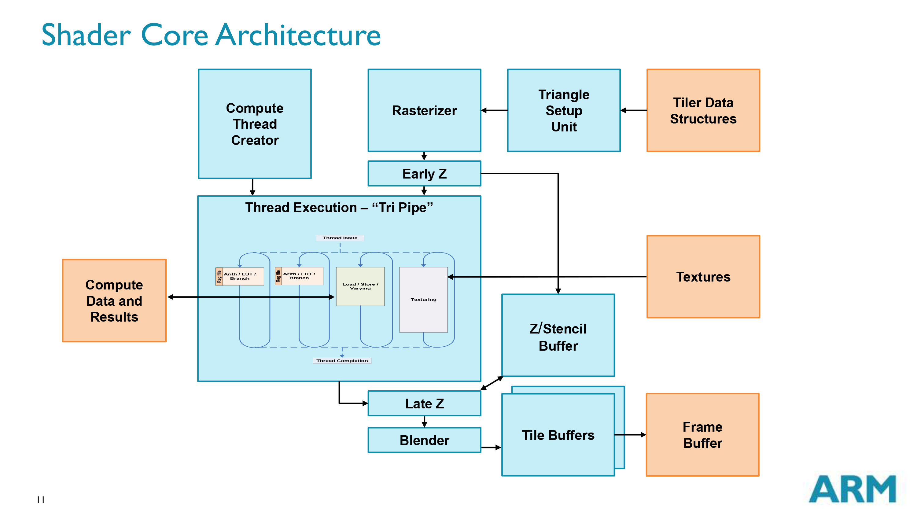
Diving in to the Mali architecture, we’ll start with a high level overview of the architecture. What we’re looking at here is a single Midgard shader core, which despite the “shader” name actually contains a whole lot more. A shader core in this context contains the actual shader core within one of Midgard’s “tri pipe” shader blocks, but also contains a triangle setup unit, rasterizer, Z & stencil hardware, a ROP/blender, tiling hardware, and a compute thread creator specifically for feeding a tri pipe with compute workloads.
Midgard – and Mali-T760 in particular in our case – is designed to scale up and down in performance and size on the basis of these shader cores. While they contain a large part of the hardware for a GPU, they are not on their own a complete GPU. They are instead designed to be laid down in multiples, and then fed by a collection of supporting hardware to make a complete GPU. This combination of shared hardware and scalable core counts allowing Midgard designs to scale from single cores up to a huge 16 cores in the largest Mali-T760MP16 configuration.
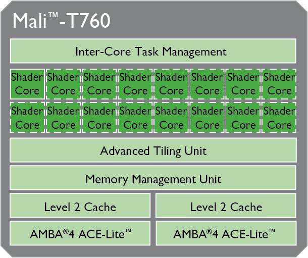
The shared hardware in Midgard is primarily concerned with managing the interaction of the shader cores, followed by providing the L2 cache and all further memory interfaces for accessing main memory and/or the CPU cache. In the case of Mali-T760 there is 1 task management unit and memory management unit, but 2 sets of L2 cache and the AMBA interface that connects the GPU to the rest of the system.
Jumping back to the core itself, let’s talk about the tri pipe for a bit. We’ll discuss arithmetic and thread execution on the next page, but from a high level a tri pipe is composed of one or more ALU blocks, a load/store unit, and a texture unit. From a high level the inclusion of ALUs, load/stores, and texturing in a single block is fairly typical for a GPU. However the variable number of ALU blocks is uncommon for a GPU. Many GPU designs maintain the same structure throughout and replicate what amounts to the tri pipe, rather than varying the number of units in the tri pipe itself.

As we’ve stated before, for our purposes we’re primarily looking at the Mali-T760. On the T760 ARM uses 2 ALU blocks per tri pipe, which is the most common configuration that you will see for Midgard. However ARM also has Midgard designs that have 1 ALU block or 4 ALU blocks per tri pipe, which is one of the reasons why seemingly similarly GPUs such as T760, T720, and T678 can look so similar and yet behave so differently.
| ARM Mali Midgard Arithmetic Pipeline Count (Per Core) | |||
| T628 | 2 | ||
| T678 | 4 | ||
| T720 | 1 | ||
| T760 | 2 | ||
Without being fully exhaustive, among various Midgard designs T628 and T760 are 2 ALU designs, while T720 is a 1 ALU design, and T678 is a 4 ALU design.
As one would expect, the different number of arithmetic pipelines per tri pipe has a knock-on effect on performance in all aspects, due to the changing ratio between the number of arithmetic pipelines and the number of load/store units and texture units. T678, for example, would be fairly shader-heavy, whereas the 2 ALU designs strike a closer balance between shading and texturing. Among the various Midgard designs ARM has experimented with several configurations, and with the T700 series they have settled on 2 ALU designs for the high-end T760 and 1 ALU for the mid-range T720 (although ARM likes to point out that T720 has some further optimizations just for this 1 ALU configuration).
In any case, each arithmetic pipeline is independent, working on its own set of threads. This is unlike some superscalar architectures, where additional arithmetic pipelines would be used for the execution of further non-blocking instructions in a thread.
The texturing unit meanwhile fairly simple. Midgard can process 1 bilinear filtered texel per clock, or 1 trilinear filtered texel over 2 clocks (to account for the second mipmap access). Note that the number of texture units and the number of ROPs per shader core is identical in the case of our T760, so in any core configuration there is a 1:1 ratio between texels and pixels.
Meanwhile, on one final stop while we’re looking at the functional blocks of Midgard, let’s talk about what we don’t see: a tessellation block. As we discussed before Midgard will support tessellation – T760 even supports Direct3D FL 11_1 – but nowhere will you see a tessellation block in the Midgard architecture.
As it turns out this isn’t an oversight or purposeful omission on ARM’s part, but rather an intentional design choice for Midgard. Midgard is fully capable of tessellation, it just does so without a fixed function unit to handle the geometry creation process.

Overview: Fixed Function Tessellator
In lieu of that Midgard implements tessellation on its shader hardware. Not just the hull and domain shader stages, mind you (which are done on shader hardware anyhow), but the actual geometry generation takes place there too. This is without a doubt a highly unusual situation, as we have never seen a tessellation-capable GPU without a dedicated tessellation unit thus far, making Midgard the first (and so far only) GPU we know of with such a design.
In discussing this design decision, ARM has told us that at the end of the day this choice is based on balancing the use of limited die space with benefits of a dedicated tessellation unit, and just how well the rest of the GPU can consume tessellated polygons. As it turns out the Midgard shader engine can tessellate at a higher rate than the rest of the pipeline can consume the additional polygons, meaning that a dedicated tessellation unit in the case of Midgard would not improve tessellation performance since it would be bottlenecked by the rest of the pipeline just as well. Furthermore any die space that ARM did dedicate to a tessellation unit would be die space they couldn’t dedicate to something else, such as additional shader hardware.
Ultimately whether this was the right decision or not is only something ARM can know – only they would have the simulation data for hardware tessellation versus shader tessellation – but this single omission already makes Midgard a highly unusual (and not to mention unique) GPU architecture. But from an outsider’s perspective we are left wondering what the power cost of this decision is. There’s no reason to doubt ARM’s space/performance argument, but as traditional GPU logic goes, doing anything in flexible hardware is going to be more power intensive than a highly specialized fix function unit, which is why we have so many of them in SoC GPUs and desktop GPUs alike. Performance aside, is shader tessellation significantly more power intensive than a theoretical hardware tessellation Midgard GPU? And if so, what does that do for power bottlenecking?
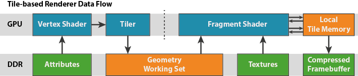
Moving on from our look at the fixed function units of the shader core to a broader execution picture, when it comes to graphics and like many other SoC-class GPUs, Midgard is a tile based architecture. This in a nutshell involves the GPU (specifically the tiler) breaking up scenes into individual tiles to be processed on a tile-by-tile basis, rather than rendering the scene at once, generally on a per-polygon basis. By breaking up a scene into tiles and then working on them one piece at a time, this allows Midgard to keep a constrained portion of the frame as the active workload, and in turn keep that tile in local memory on the GPU, rather than having to go to the slower main memory.
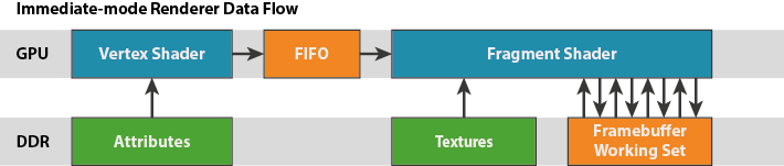
SoCs are ultimately constrained in every way possible – power, die size, and memory bandwidth – but it’s the last item more than anything else that can impact performance, making effective memory bandwidth usage especially important. Main memory accesses not only eat up valuable and limited memory bandwidth, but require burning further power to do so.
For Midgard ARM uses what they call a Hierarchical Tiling system, which as the name implies implements tiles on a hierarchical basis. The use of a hierarchy in this case allows Midgard to use variable tile sizes, based on the idea of further decomposing tiles (going down the hierarchy) until the tile complexity is at the desired size (or they’ve reached the minimum tile complexity). This ultimately allows Midgard to only use small tiles where it’s necessary, and conserve resources by working on large tiles where there is little scene complexity.

Making the best use of tiling does require some cooperation on the part of OSes and programs – Windows actually has a driver flag to indicate whether a GPU is a tiling GPU – but it offers some very important and necessary memory bandwidth optimizations for SoC-class GPUs. Making use of tiling just ultimately requires managing scene complexity to keep the tiling system and the memory footprint of the tiles under control, which is another situation of where Hierarchical Tiling flexes its muscles.
On the subject of tiling and bandwidth efficiency, Midgard also further cuts down on work and bandwidth wastage by rejecting work as early and as frequently as it can. The Early Z unit in each shader core can identify some polygons that would otherwise be covered and not visible, ejecting them before they make it to shading and texturing. And when that’s still not enough, Midgard (as of T620 and later) implements a technique called Forward Pixel Kill to further reject pixels. Forward Pixel Kill is at a basic level to pixels what Early Z is to polygons, identifying and rejecting covered pixels early enough to keep them from rendering. By keeping a small FIFO buffer and watching what pixels are being colored, Midgard can reject threads of pixels in mid-flight if it determines that the location they’re to be drawn is now covered by an opaque pixel.

Moving on, let’s talk about an area where ARM’s CPU background has come into play for their GPU designs: bitness and memory access. Developed alongside Midgard was ARM’s ARMv8 (aka ARM64) architecture. As one of the biggest design goals of ARMv8 was to extend it to a 64bit architecture, so the same choice was made for Midgard. As a result Midgard is fully 64bit; it can process 64bit Integers, double precision floating point numbers (FP64), and even natively use 64bit memory addresses. ARM wanted Midgard to be just as 64bit ready as ARMv8 would be.
The presence of 64bit operations is in and of itself fairly rare for an SoC GPU – 64bit operations are important for certain classes of compute workloads, but are seldom-to-never used for graphics operations – however ARM’s plans extend beyond just computational precision. Because Midgard can use 64bit memory addresses, Midgard can use the same 64bit address space as ARMv8 CPUs. This ability allows Midgard to achieve I/O concurrency with ARMv8 CPUs, allowing it to read directly from the CPU’s cache. Even with this Midgard and ARMv8 are not fully cache coherent – this feature is mostly about letting the GPU gorge on the CPU cache to more efficiently pass data from the CPU to GPU – but full cache coherency is coming.
In fact for as important as ARM’s decisions have been in making Midgard’s shader cores compute capable, equally as important is 64bit addressing and I/O coherency. ARM is after all a member of the Heterogeneous System Architecture (HSA) group, and has for some time now reiterated their intentions to back and invest in GPU computing both on a stand-alone basis and on a tightly integrated CPU/GPU basis. Midgard to that end is still in the stand-alone compute stage, but it incorporates optimizations that help performance right now while setting a clear roadmap towards an HSA-capable ARM CPU + GPU design. At the end of the day ARM needs to save power, and letting the GPU work on hardware-appropriate workloads is one such way to achieve this.
Finally, speaking of power let’s talk about Midgard’s power management capabilities. It would be disingenuous to merely state that Midgard is power optimized, as it implies that SoC GPUs are somehow not power optimized when in fact everyone is just as badly power bound, but going forward power consumption is only going to get more and more important as energy efficiency improvements from new fab nodes is not what it once was.
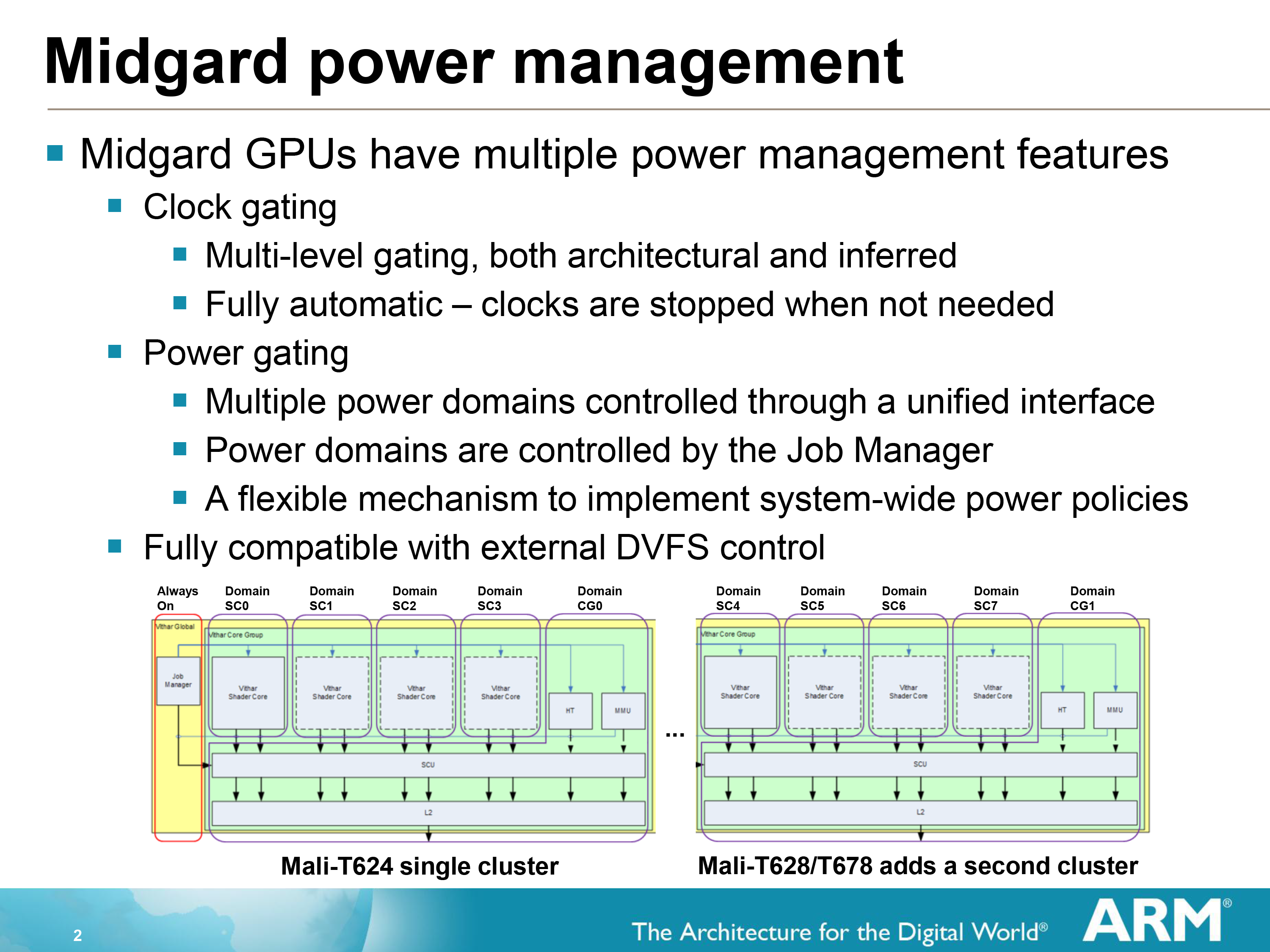
All told then, Midgard implements a number of tricks to reduce power consumption. Every rendering optimization we’ve talked about thus far is a power optimization, but on top of that Midgard implements both clock gating and finely grained power gating to either shut off power usage (or at least reduce it) for every inactive block as the situation allows. Each shader core sits on its own power domain, allowing cores to be shut down in the case of light workloads.
Even within those shader cores, the various blocks can be clock gated to bring down their power consumption. Inside the Midgard arithmetic unit the scalar and vector units can be separately clock gated, right down to the individual SIMD lanes of the vector unit itself.
Ultimately there’s only so much ARM can do to reduce power usage when a block is needed. In those cases ARM relies on achieving a balance between (relatively power hungry) clockspeeds and wide GPUs, and further utilizing workload rejection technologies to do what they can (and we’ll look at a couple more of those in a moment). But in lieu of the ability to further reduce power consumption under load, ARM is giving Midgard’s blocks a chance to rest whenever they can.


66 Comments
View All Comments
darkich - Friday, July 4, 2014 - link
You guys are missing the fact that Snapdragon 805 can reach a much higher memory bandwidth than Tegra K1.TheJian - Saturday, July 5, 2014 - link
But it still loses to K1 in most gpu stuff (all?). You're forgetting AMD/NV have had 20yrs of trying to figure out how to get the most they can from bandwidth for gaming. The devs have had that long working with their hardware also (game devs I mean). Everyone else has to play catch up here for years as they've never had to do anything game wise until last year or so as android etc gaming pumped up a bit.That is why you see ZERO Qcom optimized games (or did I miss one?) :) It's easier to optimize for a chip you already know inside out (amd/nv). I even went to Qcom's gaming page just to see if there were any games they had on their list that were REQUIRING snapdragon to see xx effects etc. There were none last I checked. All the games are just on googleplay with no snapdragon mention (like on NV games they say THD, and these games look quite a bit better than the regular versions) as they appear to work on ALL players chips. Google seems to be realizing K1 is where you want to be on gpu's at least for gaming centric stuff/automotive and I'd expect devs to continue to favor NV for optimizations as they don't need to learn a thing about k1 it's KEPLER which they've already spent 2yrs+ playing with (probably longer as they get dev versions long before we get a retail card so games can be made/optimized for them by the time they hit).
At 20nm xbox360/ps3 will be left behind as new games keep getting made on mobile. If you're not on xbox1/ps4 you'll be buying some cheap 20nm console box that has cheap games ($2-20 vs. $60 for xbox1/ps4) and as good or better graphics than last gen xbox360/ps3. GDC 2013 & 2014 surveys show devs are already massively making games for mobile and as 20nm kicks in everyone has K1 power levels or more. These android consoles/tv's etc will have more tricks than those ancient consoles so you should be able to get much better gaming experience on them for $100-200. The games pricing alone is a draw for poor people. With the ports happening right an left now of quality PC/console games and super cheap pricing there is even more reason to run to mobile for poor people who never played them before (half-life2, trine2, Serious Sam3BFE, none sold more than 11mil or so). There are a billion android users and most clearly have played none of this stuff even the console ports like Final Fantasy games, GTA games etc (on or off PC also doesn't matter) haven't been played by more than 10mil or so combined each. Lost of great stuff for poor people to pick up for under $10 in ports until the REAL new games for mobile hit this xmas/next xmas. All of the stuff the dev surveys show they've been working on will hit this year or next, and they are not angry birds games.
przemo_li - Tuesday, July 8, 2014 - link
Alternative view on Google stance:Nvidia is just first vendor that allowed them to show more features than are possible on Apples A7.
(Mobile-only vendors are not interested in full OpenGL...)
TheJian - Sunday, July 6, 2014 - link
If they're worried about lawsuits (odd they'd say that without merit), they must have had their lawyers tell them they'd be sued due to stealing tech that is probably from AMD/NV. DMCA takedowns, completely closing the kimono so to speak shows they are afraid for good reason. It isn't just competitor crap as nobody else is afraid of that it seems. The same tricks are being used by almost everyone to a large degree. So it seems to me they clearly owe someone some money and don't want to pay. They will probably show their details once they remove that stuff from a future gen soc or never I guess if they just can't remove it for some reason :)mczak - Thursday, July 3, 2014 - link
You could add Intel HD graphics (baytrail) though. Also quite interesting architecture-wise imho.btw some small correction wavefront size for amd (gcn) is 64, not 16 (I think this was wrong on older anandtech articles too). The simd size is 16 indeed but the same instruction is executed for 4 clocks always (on 16 different elements of the wavefront each clock).
mczak - Thursday, July 3, 2014 - link
Here's actually an explanation how the wavefront size of 64 works for gcn:http://devgurus.amd.com/thread/168154
Achtung_BG - Thursday, July 3, 2014 - link
My first touch phone is black LG Viewty in 2008 with Mali GPU :) :) :) If you have new article for android extention pack comparison with full Open GL will be very intrasting.Jedibeeftrix - Thursday, July 3, 2014 - link
yes please.i'd like to know:
1. how long until the AEP is rolled back into what will be OpenGL ES 4.0
1.1. whether it represents a subset of an existing OpenGL full-fat version (eg 4.4)
2. how this compares to DX 11.2 feature wise
2.1. whether AEP will be expanded in OpenGL ES 4.0 to make it broadly DX 11.2 compliant
przemo_li - Tuesday, July 8, 2014 - link
1) Never. (Though, separate extensions, can get into ES. AEP is just thin bundle over many other extensions)1.1) Yes. OpenGL 4.x is still capable of running AEP code.
2) DX11.2 is single vendor en-devour currently... (And You really should compare to F(eature)L(evel)11_2).
2.1) WHY?
Why on earth You need all those things?
Industry move in different direction. (Mantle, DX12, Metal, AZDO)
Doing stuff efficiently is new mantra now.
Adding more stuff from DX FL11_2 (Yes if You talk about features You MUST use F(eature)L(evels)!!!), would only complicate things for OpenGL ES.
We need AZDO.
Kevin G - Thursday, July 3, 2014 - link
I can see Qualcomm's concerns about a shader arms race in mobile: it has already happened on the CPU side without much benefit to the consumer. However, with the explosion in screen resolution in tablets, a spec race here would have a more tangible benefit for consumers. It sitll boggles my mind that a retina iPad has 50% more pixels and a slower GPU than my desktop system with a 1080p monitor driven by a GTX 770. My sole concern would be temperatures and power consumption.Well if Qualcomm isn't going to disclose the information, how much can be implied from driver information? Qualcomm purchased the mobile Radeon drivision from AMD back in 2009 and then came up with the anagram Adreno. If they're still using a design based upon what they got form AMD, it'd be reflective in similar drivers. If they've come up with a new architecture, it too would be evident in radically different drivers. The details would be lacking of course but some generalities could be made.