ARM’s Mali Midgard Architecture Explored
by Ryan Smith on July 3, 2014 11:00 AM ESTTricks of the Trade: Transaction Elimination and Frame Buffer Compression
While we have spent some time covering various techniques ARM uses to improve efficiency in Midgard, we wanted to spend a bit more time talking about two specific techniques in general that we find especially cool: transaction elimination and frame buffer compression.
Going back once again to what we said earlier about rendering and power efficiency, any rendering work ARM can eliminate before it’s completed not only improves performance by freeing up resources, but it also frees up power by not having to spend it on said redundant work. This is especially the case for anything that wants to hit system memory, as compared to the on-die caches and memories available to the GPU, system memory is slow and expensive to operate from a power perspective.
For their final two tricks then, having already eliminated as much rendering work as possible through other means, ARM’s last tricks involve minimizing the amount of data from rendered tiles and pixels that needs to hit system memory. The first of these tricks is Transaction Elimination (TE), which is based on the idea that if a scene (or parts of it) do not change, then it makes no sense to spend power and bandwidth rewriting those identical screen portions.
![]()
To accomplish this, ARM relies on their tiling system to break down the scene for them, and from there they can begin comparing tiles that are waiting for finalization (ROP/blending) to the tiles that are already in the frame buffer from the previous frame. Using a simple cyclic redundancy check to compare the tiles, if the tile to be rendered is found to be identical to the tile already there, the tile can be skipped and the memory bandwidth saved. Altogether of all of ARM’s various tricks, this is among the simplest conceptually.
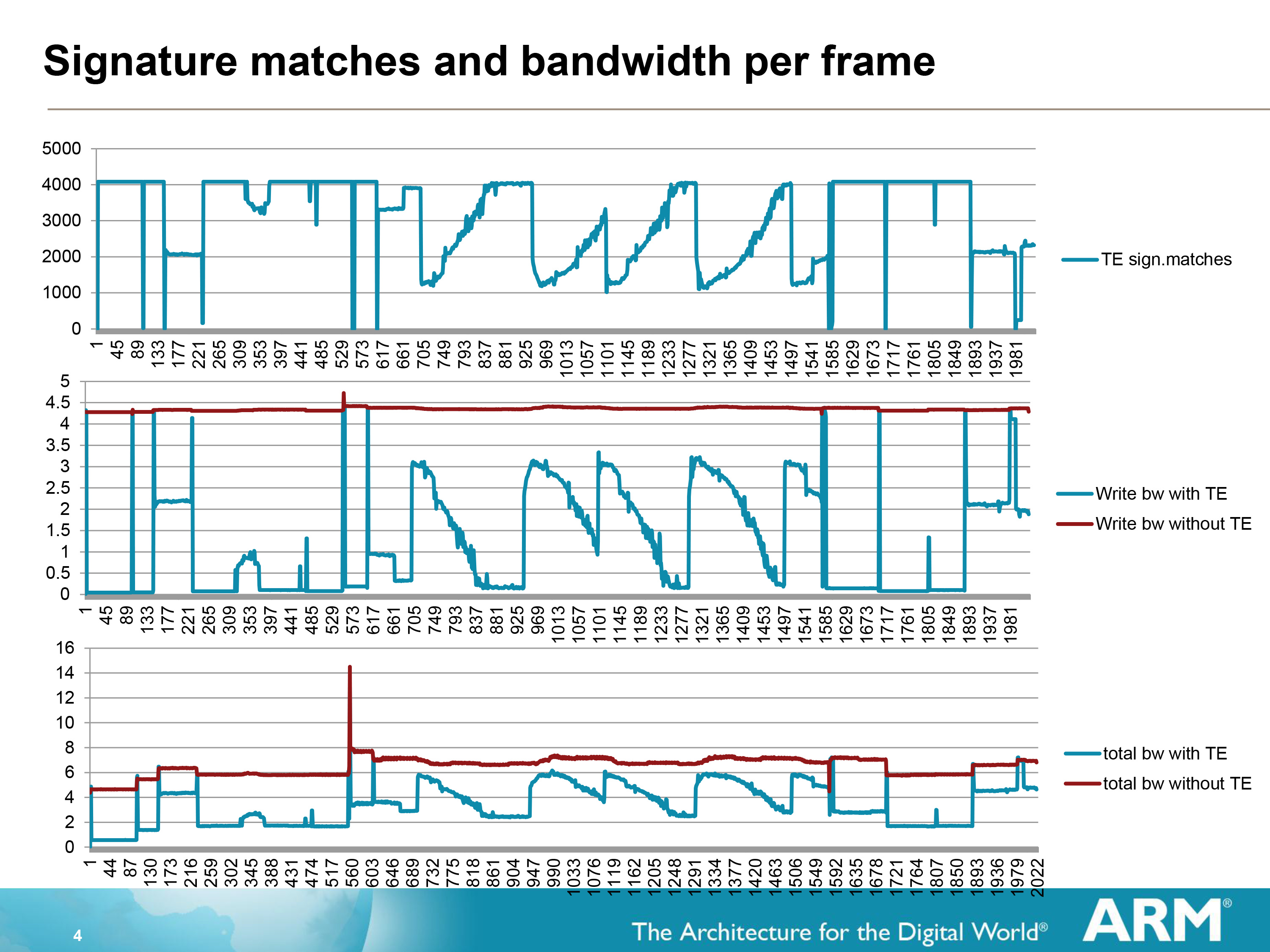
The effectiveness of Transaction Elimination in turn depends on the content. A generally static workload such as a movie will have a high degree of redundancy overall (notably when the camera is not moving), while a game may have many moving elements but will still have redundant elements that can be skipped. As a result ARM can save anywhere between almost nothing and over 99% for a highly static workload, with the average more than offsetting the roughly 1.5% overhead from computing and comparing the CRCs.
Of course Transaction Elimination does have one drawback besides its low overhead, and that is CRC collisions. During a CRC collision a pair of tiles that are different will compute to the same CRC value, and as such Transaction Elimination will consider them identical and throw away the new tile. With a standard CRC value being 64bits, such a collision is rare but not impossible, and indeed will statistically occur sooner or later. In which case Transaction Elimination has no fallback method; it is judge, jury, and executioner as it were, and the new tile will be lost.
As a result Transaction Elimination is interestingly imprecise in a world of precision. When a collision occurs the displayed tile will be wrong, but only for as long as there is a collision, which in turn should only be for 1 frame, or 1/60th of a second.
Moving on, when worse comes to worse and ARM does need to write a new tile, on the Mali-T700 series GPUs they can turn to ARM Frame Buffer Compression (AFBC) to minimize the amount of memory bandwidth they spend on that operation. By using a lossless compression algorithm to write out and store a frame, memory bandwidth is saved on both the writing of the frame and in the reading of it.
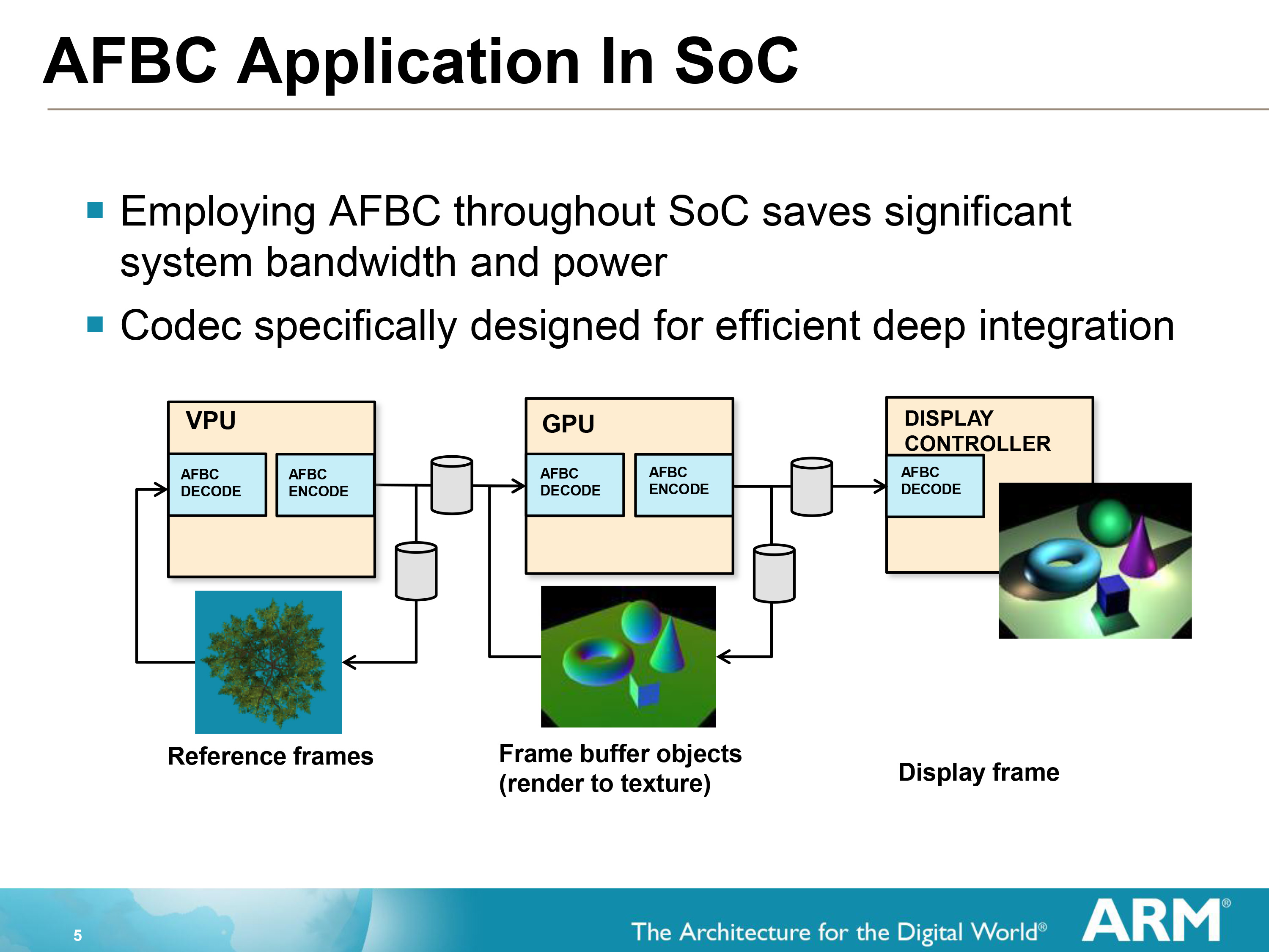
AFBC requires that both the GPU and the Display Controller support the technology, as the frame remains compressed the entire time until decompressed for display/consumption. Interestingly this means that the GPU needs to be able to compress as well as decompress, as it can reuse its own frames either in frame buffer objects (where a frame is rendered to a texture) or in Transaction Elimination. This becomes a secondary vector of saving bandwidth since it results in similar bandwidth savings for the frame even if the frame is never touched by the display controller itself. A similar principle applies to ARM’s video decoders (VPUs) which can use AFBC to compress a frame before shipping it off to the GPU.
On that note, it’s worth pointing out that while AFBC is an ARM technology, for interoperability purposes ARM does license it out to other display controller designers. ARM puts together their own display controllers, but because SoC integrators can use one of many display controllers it’s to ARM’s own benefit that everyone else be able to read AFBC as well as ARM can.


66 Comments
View All Comments
LemmingOverlord - Thursday, July 3, 2014 - link
Quick suggestion: considering Adreno is one of the most widespread GPU architectures for mobile, could you edit the table in the last page to include Adreno 3xx/4xx GPUs?Thanks!
Anand Lal Shimpi - Tuesday, July 8, 2014 - link
Unfortunately Qualcomm refuses to disclose much detail about their GPU architectures. I completely disagree with their position and have worked on Qualcomm for years to get them to open up but at this point it's a meaningless effort.da_asmodai - Thursday, July 3, 2014 - link
How about adding the Qualcomms Adreno 420 to the comparison.Anand Lal Shimpi - Thursday, July 3, 2014 - link
I wish we could - Qualcomm refuses to disclose any deeper architectural details about any modern Adreno GPU architectures.Krysto - Thursday, July 3, 2014 - link
Their loss. Plus, neither Adreno 420 nor their upcoming CPU's look that interesting or competitive anyway. Adreno 420 should still give only about HALF the performance of Tegra K1's GPU.ChefJeff789 - Thursday, July 3, 2014 - link
Really? That's disappointing... I'm really looking forward to a time when ARM, nVidia, and AMD all compete on an architectural level in their GPUs, if it ever comes. The one-horse race with Intel in the desktop CPU space has been pretty lackluster for the past few years, in terms of performance increases. nVidia's Maxwell architecture seems pretty amazing in terms of efficiency, and I'm not yet convinced AMD will be able to compete. They have yet to impress with their APU and mobile processor efficiencies.frostyfiredude - Thursday, July 3, 2014 - link
Important to note that NVidia's TK1 will be achieving that double GFLOPS performance of the Adreno 420 at a clock speed of around 950Mhz. At that performance level the TDP is listed at <10W, so it's not exactly comparable to the S805 and Adreno 420 which target a TDP half as high. What I can see happening is the TK1 being able to stretch it's legs and thus being superior in large tablets but being too thermally crippled in phones and small tablets to reach those levels. Based on the previews I found, Adreno is more efficient in it's shader resource usage, closing that further.lmcd - Thursday, July 3, 2014 - link
That's actually pretty bad math there -- if the TK1 achieves double perf at double power, it should achieve the same perf at 1/4 power (well, not quite since it isn't as simple as the basic E&M I learned, but yeah).And by your logic still, why would the K1 not fit in phones and tablets even as the 420 manages?
tuxRoller - Friday, July 4, 2014 - link
Power is linear to f, but squares with V. I don't know that we can say that at half the f you can halve the V. Actually, that's almost certainly not the case, as it's not the case with any common processor tmk.tuxRoller - Thursday, July 3, 2014 - link
The adreno 420 provides around 220gflops. The 430 well then be over 300gflops. These are not counting changes in clock speed that could raise our lower performance.