An Introduction to Semiconductor Physics, Technology, and Industry
by Joshua Ho on October 9, 2014 3:00 PM EST- Posted in
- Semiconductors
- CMOS
- Physics
- Industry
- Technology
Interconnects
Finally, it’s time to talk about what lies ahead. One thing we haven’t talked about yet are the pressing issues of the near future. For example, there are major issues looming with interconnect delay that haven’t been solved yet. As we discussed in BEOL processing, the current system of wiring these metal layers uses copper with a dielectric in between the wires with a tantalum/tantalum nitride cap to support the next layer. However, the smaller the wires get, the worse electron mobility becomes.
This is roughly analogous to the issues that we see in the front end of line, which saw decreasing drive current for the same reasons. Combined with the capacitance produced between wires, there is dramatically increasing RC time delay in the connections made between transistors that hurts performance due to lower peak clock speeds. Ultimately, progress can only be made on this end by using lower k dielectrics and lower resistance materials to drive down both resistance and unwanted capacitance in these circuits.
Next Generation Lithography
There’s still more to talk about though. While we’ve managed to stretch 193mm immersion lithography further than anyone ever imagined, 10 nanometers is likely to be the end of the road for 193nm. Here, the future is unclear. Realistically, it seems that there are only a few techniques that will be viable at the next level. These include extreme ultraviolet lithography (EUVL), nanoimprint lithography, and electron beam lithography. Let's go over each one to try and understand what challenges are coming and which option may be the best in the long run.
EUV
On the surface, EUV is a relatively straight progression of the current 193i deep-UV (DUV) technology and should deliver the significant jump needed to advance lithography beyond 10 nanometer feature sizes. While this seems easy enough, there are a large number of issues that crop up from such a short wavelength (~13nm) of light.
First, the EUV light source itself is no longer a laser in most cases. This means that the energy efficiency of the light source is extremely low compared to current 193nm excimer lasers, and as a result an enormous amount of energy has to be used to generate an incoherent light source that is then filtered to only produce EUV.
Second, EUV is strongly absorbed by almost all matter. This means that the lithography must take place in a vacuum, which rules out techniques such as immersion lithography to further resolution enhancements. By using a strong vacuum for lithography, the amount of wafers that can be processed per hour drops dramatically as vacuuum chucks can no longer be used to hold the wafer, and the electrostatic chucks used must be heated to a stable temperature with a sacrificial wafer. Also, keeping the wafer heating from the EUV exposure becomes a significant issue because the immersion fluid that once cooled the wafer cannot be used.
In addition, it's impossible to use transmissive lenses because of this same issue. As a result, mirrors must be used to focus and reflect the EUV light on to the target. There are potential issues with EUV damaging the mirrors in the optical system, and in order to reflect the EUV light all of the mirrors and the photomask have to be coated with multiple layers that use interference effects to maximize reflected light. This also means that even minor defects in a photomask can result in an unusable photomask, as seen in the photo below.
Buried Defect on EUV Mask Blank / Guiding light / CC BY SA
Unfortunately, these defects cannot be seen using an electron microscope. In order to see these defects, an EUV microscope must be used. Outside of these challenges, EUV itself intrinsically has multiple issues that reduce resolution in some unexpected ways. First, shot noise becomes a serious issue. What this means is that it's fundamentally impossible to completely control the number of photons that are released into the photoresist. This means that the lines drawn by an EUV can be unacceptably rough unless enough photons are used to ensure that shot noise is statistically insignificant, but this only increases the power requirements for EUV lithography. To make things worse, by increasing the amount of exposure to the photoresist the material can be damaged by the sheer intensity of the heating effect of EUV.
Finally, because EUV is so energetic, it is a form of ionizing radiation. This means that when EUV light is absorbed by a molecule, electrons can be liberated. Unfortunately, this adds yet another source of uncertainty and also decreases resolution because the generated photoelectrons move randomly through the photoresist. In effect, all of these issues reduce the true resolution of EUV to somewhere around the 15-19nm feature size for a single exposure. In order to even get to 10nm and below, double patterning is required to reach the resolution necessary.
In short, the resolution gain from current 193nm technology is relatively small compared with the enormous expense and new design challenges. Based on how many delays have occurred with the introduction of EUV lithography, it may mean that a radically new system is needed to fabricate even smaller ICs. That's where nanoimprint and e-beam lithography come in.
Nanoimprint Lithography
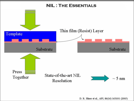
Nano Imprint / UMD
This type of lithography is incredibly simple. This method is simply using a thermoplastic polymer coated onto the substrate (such as a silicon wafer), and then a mold is pressed down on the wafer to print a pattern. Once this is done, a pattern transfer technique such as plasma etching is used to etch away the resist as necessary to expose the pattern on the wafer.
While this technique is simple and can easily be used as a next generation lithography tool, there are also a number of flaws involved with this process. If the imprinting isn't done in a vacuum, there is a high likelihood that the mold will have air bubbles that alter the pattern in unpredictable ways. In addition, the template is susceptible to wear and tear, which means that resolution is lost as the mold is repeatedly used in imprinting. The imprint mold must also take into account uneven depth of imprinting based on the density of the pattern used and potential stretching of the resist. Finally, making the template itself requires extremely precise lithography, which means that it's limited by current generation lithography techniques in resolution. This isn't a solution by itself, which means it can only be used in conjunction with other methods.
Electron Beam Lithography
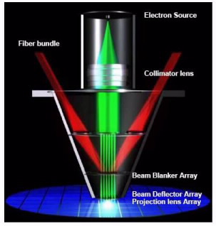
Electron Beam Lithography / SEMI
Just as we saw in the progression of microscopes, the early days were mostly focused on improving light microscopy with higher NA lenses and oil immersion, but today some of the highest resolution microscopes use electrons instead of photons. Similarly, electron beam lithography can generate some of the highest resolutions possible out of all the lithography techniques we've discussed in this article. This means that sub-10nm resolution is easily achieved. In fact, it's fully possible to do away with the resist and simply write the pattern directly on the silicon wafer, eliminating the resist as a potential bottleneck for resolution.
Unfortunately, this system is extremely slow. Rather than the 100+ wafers per hour of current photolithography techniques, electron beam lithography is often limited to less than ten wafers per hour. Using a single electron beam to write an entire 300mm wafer would take around 22 years. While thousands of beams can be simultaneously writing to the wafer to speed up the process, the electrons begin to affect the trajectory of other electrons in other beams. This requires complex modeling to compensate for such effects.
As with EUV lithography, shot noise becomes a significant issue despite a much easier ability to control the dose. This is because even small variations in the number of electrons can significantly effect the roughness of the lines drawn by the electron beam. There is also a strong need to choose a balanced energy for the electron, as excessively energetic electrons can cause significant secondary electron generation, but too little energy means the electrons are easily scattered. Both reduce resolution and can result in unacceptable defects for smaller process nodes.


77 Comments
View All Comments
Kidster3001 - Wednesday, October 29, 2014 - link
Modern chips are connected with a C4 process (Controlled Collapse Chip Connect) The interconnect side is down, the bulk side is up. The heatsink is touching the back of the wafer.nand - Friday, October 10, 2014 - link
when i was 18 and in college i couldn't get head my over this stuff - after few years of growing up it makes perfect sense...sammycbvb - Friday, October 10, 2014 - link
Awesome article. I was waiting for a simplified explanation of Semiconductors and you've delivered.GT69 - Friday, October 10, 2014 - link
Great article for this old EE whose career was mostly in sales and marketing, but who has had a great love for PC's since the days of Apple II and CP/M. Nice that someone has taken the time and effort to give this generalized explanation even if some of the nit-pickers quibble over a typo or some specific detail. Until one has had to actually produce such a piece he/she should refrain from too much criticism. Easy and quick it ain't! Kudos...Dr.Neale - Saturday, October 11, 2014 - link
After many years of editing scientific / technical / medical journal articles, I tend to see the structural details as well as the informational content.To me, a typo is like a dead pixel. If it can be removed, it makes the image or storyline that much more immersive and enjoyable to behold.
The purpose is aiding the author in polishing the article to perfection, not fault-finding or nit-picking.
Like many tech enthusiasts, an editor brings a passionate pursuit of excellence to his craft and to his team.
Like many other commenters here, I see myself as making a small contribution, from time to time, to the AnandTech team.
Dr.Neale - Saturday, October 11, 2014 - link
P.S. I have also authored or coauthored numerous articles (and a textbook chapter) in the fields of medical physics and medical imaging, including invited review articles.So I offer my appeciation and congratulations to Josh Ho for gifting us with an article of such surpassing excellence.
dew111 - Friday, October 10, 2014 - link
This was a good review of my semiconductor physics course. But with less math :)Arnulf - Friday, October 10, 2014 - link
Very nice technical article, unlike the usual consumerist Apple et al chaff that has swamped this site as of lately!Senti - Friday, October 10, 2014 - link
Exactly my thoughts! It's really sad to see how level of this site has dropped significantly over years due to caring for more mindless crowd; certain reviewers doesn't bother to actually understand what they are reviewing and just pushing for faster time to post and more numbers (that are by large part are quite unrelevant).But articles like this show that hope is not lost here – great job, would love to see more articles like this.
SanX - Friday, October 10, 2014 - link
This is what puzzling for a long time: the wavelength of ArF laser is 192nm, the feature size of Core M processor is 14nm or 14 times smaller. With NA=1 you can focus into spot of the Airy size equal approximately to wavelength only. Using phase shift trick you can probably drop that size twice to 96nm. Using nonlinearity of photoresist you can drop twice more or to 49nm. My guess is that using titlting of laser (i do not get how it actually works) they can get 24nm. Adding water you can get 24 / 1.33=18nm. How they get 14nm and sometimes even 10nm what Samsung claims with just the optical lithography?