An Introduction to Semiconductor Physics, Technology, and Industry
by Joshua Ho on October 9, 2014 3:00 PM EST- Posted in
- Semiconductors
- CMOS
- Physics
- Industry
- Technology
Light Sources
While many other technologies are tangentially related to shrinking feature size, one of the primary ways within the past four decades or so has been through smaller wavelengths of light. Shorter wavelengths mean higher resolution, much like how the electron microscope’s shorter de Broglie wavelength increased resolution over light microscopes. Thus, photolithography can increase in resolution by using light sources that generate shorter wavelengths.
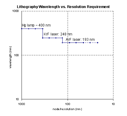
Lithography Wavelength vs Resolution / Guiding light / CC BY SA
This progression has happened steadily over the years, starting with mercury lamps that produced UV light of around 400 nanometers. Once this was no longer sufficient, lasers became necessary in order to drive higher resolution and rate of production. The first was the krypton fluoride laser that generated a wavelength of 248nm, then argon fluoride to generate 193nm. Unfortunately, this is near the limit of what can be realistically used in an environment that contains air, as even 193nm is attenuated significantly. As seen in the photo below, in order to go lower for EUV and similar wavelengths, the lithography process must be done in a vacuum as otherwise air will absorb almost all of the energy emitted.
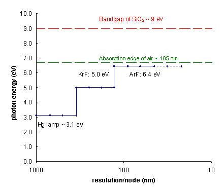
Photon Energy vs. Resolution / Guiding light / CC BY SA
Immersion Lithography
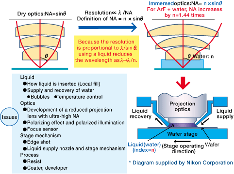
Immersion Lithography / Renesas
So the inevitable question is what could be done next. While different foundries adopt technologies at different times, one way to push resolution further is immersion lithography, which was done around the 65nm node to 32nm node. This is relatively simple, as what this effectively does is increase the numerical aperture of the optical system because the light from the source can be refracted better than before. This is done by immersing the wafer and projection lens in extremely pure water.
Of course, this is far from a simple task in practice. The deionized water must also have no gases present that could cause air bubbles between the lens and wafer, with extremely consistent temperature and pressure. Otherwise, the actual index of refraction in the water will change unexpectedly and cause defects in the lithography process. The 193nm light used in current lithography processes can also ionize the water and in turn cause reactions with the photoresist.
Unfortunately, with processes like EUV lithography it’s no longer possible to use this method to drive higher resolution and smaller feature size because the liquid used will generally absorb all of the energy emitted. However, it’s still possible to drive higher resolution with 193i technology by using fluids with a higher index of refraction, which is an area of exploration for further resolution increases.
Multiple Patterning
Multiple Patterning / SPIE
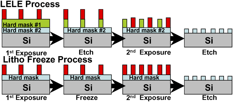
Another technique that can be used with EUV lithography is multiple patterning. While it’s “one” technique, the ways to implement multiple patterning are numerous. All have the same goal though. In essence, if a theoretical system can only provide sufficient resolution to draw two lines 64nm apart, it’s possible to double the resolution by printing another two lines 64nm apart by doing a second exposure. The result is four lines that are 32nm apart. There are a few ways to achieve this, which are known as litho-etch, litho-etch (LELE), litho-freeze, litho-etch (LFLE), and self-aligned double patterning (SADP).
LELE is rather simple in implementation and relies upon two separate photoresist layers. In the first pass, lithography is done on a hard mask, then developed. It’s important to use a hard mask, because in the second pass another layer of photoresist is applied, then exposed and developed. If there wasn’t a hard mask, the first pass would simply disappear when the second layer of photoresist is applied. LFLE is simply a modification of the LELE technique, where the hard mask is eliminated. After the initial lithography process, the photoresist is frozen by coating it with a chemical agent that is then baked and developed away, making it so that the first resist layer is separable from the second layer. Once this is done, a standard lithography pass is done to complete the process.
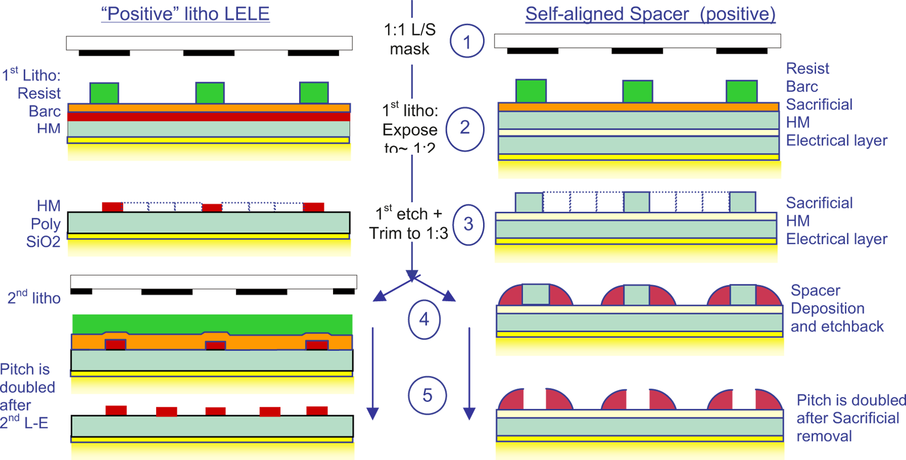
LELE & SOAP Patterning / SPIE
SADP is a very different way of doing things, but the end result is the same. The first step is doing a lithography/etch of dummy patterns that become the actual lines that are intended to be etched on the final pattern. Once this is done, a hard mask or similar material is deposited over the dummy patterns. After this, the hard mask is etched to expose the sidewalls that line the dummy patterns. Once all of this is completed, the dummy pattern is developed away and the exposed oxide is etched as usual. The result is that the lines are twice as close as before, and only one lithography pass was needed.
Unlike LELE and LFLE, there’s no need to be concerned about alignment because after the dummy pattern is set up, there’s no second exposure. This may be the reason why Intel's 22nm FinFET uses this process. Because the sidewall spacers are often created with hard mask materials, the resulting lines are also cleaner. This fact will become important, especially when discussing EUV and similar next generation lithography techniques.
While these techniques may sound like the perfect way to increase resolution, ultimately multiple patterning becomes increasingly expensive and difficult, especially because even a small misalignment between the two patterns can result in a wasted wafer. Multiple patterning also causes design restrictions that wouldn't occur with a true resolution increase in the lithography process because certain patterns become impossible with even order or odd order patterning processes.
Computational Lithography

Phase Shifting Mask / Stanley H. Chan
While we’re still talking about (relatively) low hanging fruit, I want to cover two other methods that are used to enhance resolution. The first is phase shifting masks. Rather than focusing upon wafer-level changes, this improves the reticle/mask itself. In short, this exploits the wave nature of light. There are two types of phase-shifting masks, and the first is an alternating phase-shift mask. This alters the thickness of the mask in some regions, which induces a phase-shift on the light waves that pass through it. As a result, there is interference with light from unmodified regions, which means that higher contrast can be achieved between the exposed and unexposed regions. The other type is the attenuated phase-shift mask, which only lets small amounts of light pass through that can interfere with the light coming from transparent regions.

Source Notes: Intended pattern in blue, OPC-corrected in green, final pattern in red.
Optical Proximity Correction / LithoGuy
The second is optical proximity correction, or OPC. One of the imperfections in the lithography process that we haven’t talked about until now is that what is drawn on the photomask/reticle is not translated exactly on to the photoresist. In reality, line widths vary greatly depending upon how dense the pattern around the line is; lines don’t end where they do on the mask, and the ends of lines are much thicker than the middle. OPC compensates for all of these effects and computes the photomask needed to achieve a layout close to the intended design.
Review
Summarizing things again, there are multiple techniques used to increase resolution to fabricate smaller transistors. By using lower wavelengths of light, multiple patterning techniques, and computational lithography techniques like phase shifting masks and optical proximity correction, we’ve managed to make it all the way down to 22 nanometer feature sizes. With the launch of Intel's Core M, we’ve made another jump down to 14 nanometers using the same light source that we did at 90 nanometers.


77 Comments
View All Comments
Kidster3001 - Wednesday, October 29, 2014 - link
Modern chips are connected with a C4 process (Controlled Collapse Chip Connect) The interconnect side is down, the bulk side is up. The heatsink is touching the back of the wafer.nand - Friday, October 10, 2014 - link
when i was 18 and in college i couldn't get head my over this stuff - after few years of growing up it makes perfect sense...sammycbvb - Friday, October 10, 2014 - link
Awesome article. I was waiting for a simplified explanation of Semiconductors and you've delivered.GT69 - Friday, October 10, 2014 - link
Great article for this old EE whose career was mostly in sales and marketing, but who has had a great love for PC's since the days of Apple II and CP/M. Nice that someone has taken the time and effort to give this generalized explanation even if some of the nit-pickers quibble over a typo or some specific detail. Until one has had to actually produce such a piece he/she should refrain from too much criticism. Easy and quick it ain't! Kudos...Dr.Neale - Saturday, October 11, 2014 - link
After many years of editing scientific / technical / medical journal articles, I tend to see the structural details as well as the informational content.To me, a typo is like a dead pixel. If it can be removed, it makes the image or storyline that much more immersive and enjoyable to behold.
The purpose is aiding the author in polishing the article to perfection, not fault-finding or nit-picking.
Like many tech enthusiasts, an editor brings a passionate pursuit of excellence to his craft and to his team.
Like many other commenters here, I see myself as making a small contribution, from time to time, to the AnandTech team.
Dr.Neale - Saturday, October 11, 2014 - link
P.S. I have also authored or coauthored numerous articles (and a textbook chapter) in the fields of medical physics and medical imaging, including invited review articles.So I offer my appeciation and congratulations to Josh Ho for gifting us with an article of such surpassing excellence.
dew111 - Friday, October 10, 2014 - link
This was a good review of my semiconductor physics course. But with less math :)Arnulf - Friday, October 10, 2014 - link
Very nice technical article, unlike the usual consumerist Apple et al chaff that has swamped this site as of lately!Senti - Friday, October 10, 2014 - link
Exactly my thoughts! It's really sad to see how level of this site has dropped significantly over years due to caring for more mindless crowd; certain reviewers doesn't bother to actually understand what they are reviewing and just pushing for faster time to post and more numbers (that are by large part are quite unrelevant).But articles like this show that hope is not lost here – great job, would love to see more articles like this.
SanX - Friday, October 10, 2014 - link
This is what puzzling for a long time: the wavelength of ArF laser is 192nm, the feature size of Core M processor is 14nm or 14 times smaller. With NA=1 you can focus into spot of the Airy size equal approximately to wavelength only. Using phase shift trick you can probably drop that size twice to 96nm. Using nonlinearity of photoresist you can drop twice more or to 49nm. My guess is that using titlting of laser (i do not get how it actually works) they can get 24nm. Adding water you can get 24 / 1.33=18nm. How they get 14nm and sometimes even 10nm what Samsung claims with just the optical lithography?