An Introduction to Semiconductor Physics, Technology, and Industry
by Joshua Ho on October 9, 2014 3:00 PM EST- Posted in
- Semiconductors
- CMOS
- Physics
- Industry
- Technology
Introduction and Short Channel Effects
Unfortunately, it’s not as easy as simply driving resolution higher. Improving lithography is only one aspect, and as transistors get smaller and smaller previously insignificant issues become incredibly important ones. One of the biggest issues is leakage current.
I alluded to this earlier with the discussion of band structure, but electrons more closely resemble the models of quantum mechanics rather than classical mechanics. This leads to effects such as quantum tunneling, where electrons can pass through insulating layers as if there was nothing there to stop it.
While it was safe to ignore these effects at larger process nodes, the smaller we go the worse the problems get. There are five short channel effects that can be discussed, but the primary effect of interest in drain-induced barrier lowering, or DIBL. An example of the effect that DIBL has can be seen in the image below. What DIBL means is that because the channel length is so short, the voltage applied to the drain can affect the source because the drain itself acts as a capacitor due to the separation of charge.
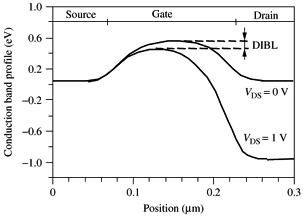
This capacitance from the drain means that the gate becomes less effective at controlling the flow of current through the gate because the drain is competing with the gate. As a result of this effect, there is a shift in the threshold voltage because the drain has made it easier for the inversion layer to be generated. When discussing threshold voltage, this generally refers to the point where current through the channel begins to increase exponentially with increases in gate voltage. In addition to this change in threshold voltage, there is a decrease in the subthreshold slope because the drain is causing a level of current to always flow through the channel. This means that more voltage has to be applied to the gate in order to generate the same increase in current flow in the channel.
It's possible to try and alleviate this issue by strongly doping the areas between the source and drain to eliminate the depletion region created. Unfortunately, another effect of this halo doping is that parasitic diode leakage increases, and due to the strong doping there is a greater scattering of electrons and lower electron mobility. In addition, because doping relies on an imperfect process, higher doping levels make the threshold voltage vary from transistor to transistor. This makes the operating voltages higher than necessary to accomodate for the variance in doping.
The end result is that performance falls off dramatically. However, there are multiple methods that can stave off these effects. These methods include straining silicon, silicon on insulator (SOI), high-k metal gate (HKMG), and FinFET.
Silicon On Insulator
Silicon On Insulator / Advanced Substrate News
One of the first methods used in this area was SOI, which will be familiar to those that followed this site 13 years ago. In short, instead of the standard bulk silicon substrate that we’ve been showing in all of our MOSFET diagrams, an insulating layer is added just beneath the channel. This is an advantage in some ways, but a disadvantage in others.
First, parasitic capacitance is reduced. What we haven’t talked about until now is that by virtue of the depletion zone and charge on the source or drain, there is a separation of charge between the source or drain and the body. A planar capacitor is nothing more than two metal plates with a dielectric between the two, with a charge on one of the plates, so this is a form of capacitance. The issue with this capacitance is that once you add a resistor in series with the capacitor, you have an inherent delay in current. This is a classical RC circuit problem, and this reduces the rate at which the transistor can switch, which reduces performance. This delay is because the rise and fall of current from switching the transistor on and off is slower than if there was no capacitance. By adding a thick silicon oxide layer underneath the transistor, the distance is increased and therefore the capacitance decreases. This means that the time delay gated by RC decreases, which means clock speed increases.
The other problem is leakage far away from the gate. In recent process nodes, leakage has become a bigger and bigger problem. This is due to the short channel effects that we discussed before. While gate-induced drain leakage (GIDL) current is one issue that arises from smaller process nodes, it's inherently a different problem. While solving GIDL is done with HKMG, channel leakage far from the gate has been a persistent issue in recent process nodes, and it's something that scaling equivalent oxide thickness (EOT) at the gate won't solve. This is because the area far away from the gate cannot have its voltage pulled down by the gate. This goes back to the effect of DIBL that we previously discussed.
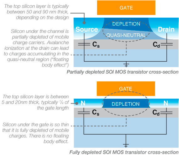
One of the first methods used to solve this problem was SOI, and by looking at a diagram of even partially depleted SOI (PD-SOI), it's clear why this is. SOI technology in general reduces the amount of silicon far away from the gate, and this in turn means that there is much less channel leakage. For PD-SOI though, because the bulk of the silicon isn't connected to a terminal the body "floats". This leads to something called the history effect, which means that the threshold voltage will change depending upon the previous voltages applied to the gate. This can also cause parasitic transistors to activate and cause leakage.
The logical conclusion to fix these issues is fully depleted SOI, which makes the channel thin enough that the body no longer floats, as it doesn't have a region where charge can accumulate one way or another. The gate can still create its inversion layer, but when the inversion layer isn't present the barrier for current is much stronger than before because all of the silicon in the channel is very close to the gate. This means that the leakage current in general is lower.
Unfortunately, SOI technology in general comes with higher cost and due to the insulating layer that the transistors are built on thermal dissipation of the transistors isn't as effective as it is on bulk processes. While AMD used to use SOI technology, they have since transitioned to bulk processes. FD-SOI is still a viable option, but for the most part SOI technology isn't found in VLSI chips like CPUs, GPUs, and other forms of digital logic. There are certainly niche cases where SOI dominates such as analog RF and radiation-hardened applications, but it seems that the foundry model makes SOI unpopular.
Straining Silicon
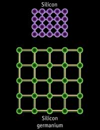
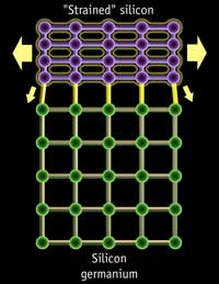
While SOI seems to have lost the popularity that it once had, other methods of improving transistor performance have become much more popular. For example, by putting silicon germanium (SiGe) or silicon carbide (SiC) in the source and drain, the silicon in the channel is stretched past its normal interatomic distance and reduces the effects of electrostatic forces. In other words, we get strained silicon. This increases the mobility of charge carriers in the channel, thus increasing drive current and overall transistor performance. There’s more than one way to achieve this, but the principle is ultimately the same. This kind of technology can be seen as early as 2003 with Intel's 90nm process.
High-k/Metal Gate
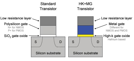
While straining silicon has been around since the 90nm node, the high-k metal gate has been critical for improving transistor performance at the 45nm node and below. When we first discussed the gate structure of a MOSFET, we talked about how a silicon dioxide layer is grown on top of a silicon substrate, which then has another polysilicon layer deposited on top of the silicon dioxide. Unfortunately, that hasn’t been the structure of the transistor gate for at least the past year for SoCs like the Snapdragon 800 and newer. HKMG has actually been around since 2007 in consumer devices with the launch of Intel’s Penryn CPUs.
The reason why HKMG is so important goes back to quantum mechanics. Those familiar with the equation for capacitance of a planar capacitor will know that reducing the distance between the two plates will increase capacitance. This means the field effect is stronger, which improves drive current and control over the channel. This control over the channel also increases the rate at which transistors switch. Unfortunately, at sufficiently small thicknesses, this all breaks down. Because electrons work probabilistically, we suddenly encounter cases where electrons begin tunneling through the insulator from the gate to the silicon channel. This causes significant leakage current through the gate to ground even when the gate isn’t being switched from one state to another, so we can no longer decrease thickness beyond a certain point.
One way to continue increasing gate capacitance while also decreasing leakage is to use a high-k dielectric, but this introduces a great deal of complexity in the manufacturing process compared to simple chemical vapor deposition of SiO2. The gate material itself can no longer be polysilicon, as it’s close enough to the inversion layer that it starts to become a depletion region. This causes issues in channel formation, so it becomes important to use a metal gate to improve performance. In addition to the poly depletion issue, a phenomenon known as Fermi level pinning occurs between the polysilicon/high-k interface. This effect dramatically raises the threshold voltage and decreases drive current.
FinFET
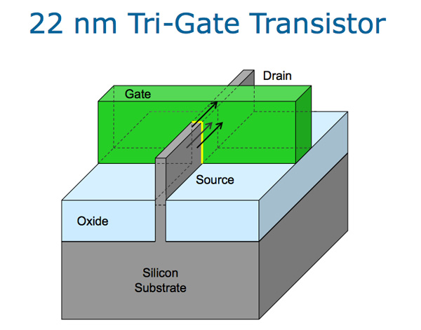
Unfortunately, once we get to 22 nanometers and below, short channel effects become even more significant. While we managed to decrease leakage and improve performance with HKMG, the gate still doesn’t have sufficient control over the channel because the gate keeps getting smaller relative to the substrate. The answer with the Tri-Gate transistor is to wrap the gate all around the channel that would form, dramatically reducing the amount of silicon far away from the gate. The resultant structure becomes like a fin, and due to the extremely thin channel the extent of the depletion region is determined by the physical structure rather than the applied bias to the terminals of the FET. This makes the transistor channel fully depleted as well, but this is merely an interesting side-effect, not a causative mechanism.
It's important to understand that this is why FinFET and FD-SOI are fully depleted technologies, but the key here is that the channel is now extremely thin so that the area far from the gate is eliminated. This means that the voltage and resultant capacitance of the gate should be able to overpower the effect of the drain's capacitance in all areas of the channel. The impact on performance is enormous.
As a result of this change, the off current is much lower than before as the effect of DIBL is reduced. This means that heavily doping the channel isn't necessary so variance in threshold voltages from one transistor to another is reduced. In addition, because of the larger inversion layer that can be generated and lower doping levels used in the channel, drive current is improved. This also means improved subthreshold swing can be achieved, so switching transistors on and off is even faster, which also improves performance. This is very much similar to the advantages that we see with FD-SOI, but it can be implemented on bulk silicon which reduces variable cost. FinFET and FD-SOI are just different ways of accomplishing the same goal, and share all the advantages of a thin channel.


77 Comments
View All Comments
DanNeely - Friday, October 10, 2014 - link
A lot of them can only make n-type or p-type transistors. While that's not a problem for power or RF transistors; to control energy consumption and heat production you need both types to do CMOS logic gates.JoshHo - Friday, October 10, 2014 - link
While GaAs is popular in MMIC applications, it normally isn't possible to implement CMOS logic with such transistors.Lux88 - Friday, October 10, 2014 - link
Thank you very much for the much needed and very well written and illustrated introduction!How long does it take in real life to make a wafer with chips (with or without the testing)? Does it take hours, days or weeks to get a finished wafer with chips from silicon crystal?
At the end you mention a rate of "100+ wafers per hour", but I understand it as "number of wafers we are working on in parallel" rather than "number of wafers from start to finish".
aicjofs - Friday, October 10, 2014 - link
Time depends on the device and fab. Weeks though. I'd guess the average for any given chip(fron latest greatest down to simple microcontrollers) 3-6 weeks in the fab, another couple for testing packaging.He was talking about replacing a single photo tool(scanner/stepper) that does 100 wafers per hour with ebeam. There can be 10-100 scanners in fab, and as you say working in parallel.
ABR - Friday, October 10, 2014 - link
Great article. Our society has poured vast resources into this area at multiple levels and achieved incredible results. I can't help but think that if we had been motivated to put this kind of engineering effort towards space projects we would not only be colonizing Mars by now, but mining asteroids and running orbital solar panels. Maybe we'll eventually come back to these things, with new powers bestowed by this "inner space" technology. Or maybe not.pepone1234 - Friday, October 10, 2014 - link
This article is amazing!! Thank you for writing this :DKhenglish - Friday, October 10, 2014 - link
You missed the biggest reason why SOI has gone out of fashion from microprocessors. Costs and fabrication are not a big deal. All you do is implant O2 deep into the wafer, then heat it to turn the implanted O2 into SiO2. This is 2 extra steps of 400 or so done when processing a wafer. No big deal.The problem is that there is no more transistor body connection to ground. This means that the body can build up charge like in flash memory. What it ends up doing is skewing the threshold voltage. When doing high voltage work with radio or power electronics with big transistors this is no big deal, but with microprocessors it is a significant. Even worse is this charge depends on the previous state of the transistor and how long it has been in that state, which is difficult to predict, and thus we have unpredictable performance swings with SOI.
JoshHo - Friday, October 10, 2014 - link
This is a PD-SOI issue that falls under history effects mentioned in the article. FD-SOI doesn't have history effects as the body doesn't inherently have mobile charge carriers, which must be generated by band-bending.Khenglish - Friday, October 10, 2014 - link
So if FD-SOI gets rid of body effects then why is SOI not common? I supposed you can't just implant O2 and anneal for FD-SOI? Is sanding the wafer and growing SiO2 what needs to be done?The article also mentions temperatures, but the heatsink is attached to the interconnect side of the CPU instead of the bulk side from my understanding so this should have no impact.
JoshHo - Saturday, October 11, 2014 - link
The biggest issue continues to be cost. While continuing to push bulk CMOS is more expensive in up-front cost, SOI has much higher fluid costs. There's also only one supplier of SOI wafers to my knowledge. (Soitec)