An Introduction to Semiconductor Physics, Technology, and Industry
by Joshua Ho on October 9, 2014 3:00 PM EST- Posted in
- Semiconductors
- CMOS
- Physics
- Industry
- Technology
Light Sources
While many other technologies are tangentially related to shrinking feature size, one of the primary ways within the past four decades or so has been through smaller wavelengths of light. Shorter wavelengths mean higher resolution, much like how the electron microscope’s shorter de Broglie wavelength increased resolution over light microscopes. Thus, photolithography can increase in resolution by using light sources that generate shorter wavelengths.
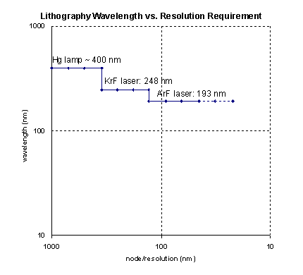
Lithography Wavelength vs Resolution / Guiding light / CC BY SA
This progression has happened steadily over the years, starting with mercury lamps that produced UV light of around 400 nanometers. Once this was no longer sufficient, lasers became necessary in order to drive higher resolution and rate of production. The first was the krypton fluoride laser that generated a wavelength of 248nm, then argon fluoride to generate 193nm. Unfortunately, this is near the limit of what can be realistically used in an environment that contains air, as even 193nm is attenuated significantly. As seen in the photo below, in order to go lower for EUV and similar wavelengths, the lithography process must be done in a vacuum as otherwise air will absorb almost all of the energy emitted.
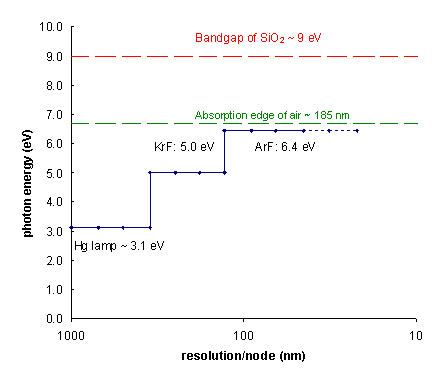
Photon Energy vs. Resolution / Guiding light / CC BY SA
Immersion Lithography
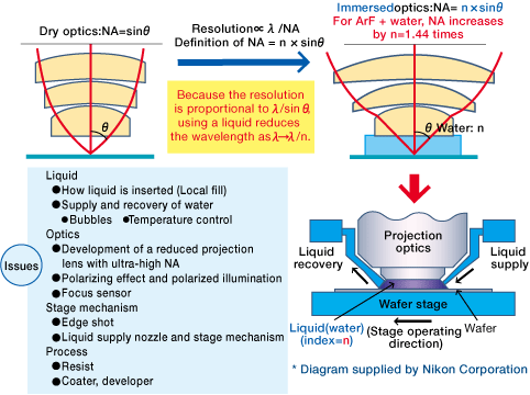
Immersion Lithography / Renesas
So the inevitable question is what could be done next. While different foundries adopt technologies at different times, one way to push resolution further is immersion lithography, which was done around the 65nm node to 32nm node. This is relatively simple, as what this effectively does is increase the numerical aperture of the optical system because the light from the source can be refracted better than before. This is done by immersing the wafer and projection lens in extremely pure water.
Of course, this is far from a simple task in practice. The deionized water must also have no gases present that could cause air bubbles between the lens and wafer, with extremely consistent temperature and pressure. Otherwise, the actual index of refraction in the water will change unexpectedly and cause defects in the lithography process. The 193nm light used in current lithography processes can also ionize the water and in turn cause reactions with the photoresist.
Unfortunately, with processes like EUV lithography it’s no longer possible to use this method to drive higher resolution and smaller feature size because the liquid used will generally absorb all of the energy emitted. However, it’s still possible to drive higher resolution with 193i technology by using fluids with a higher index of refraction, which is an area of exploration for further resolution increases.
Multiple Patterning
Multiple Patterning / SPIE
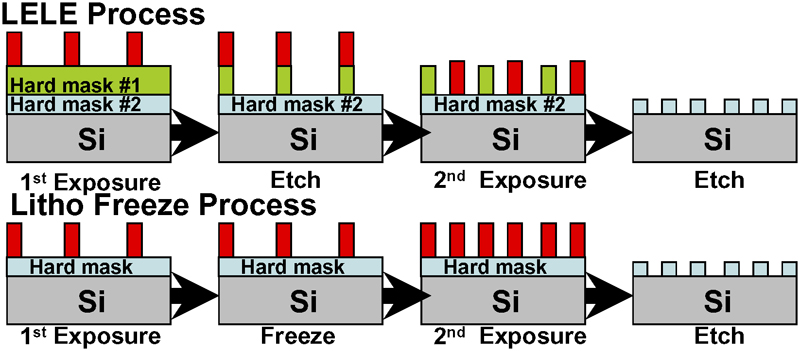
Another technique that can be used with EUV lithography is multiple patterning. While it’s “one” technique, the ways to implement multiple patterning are numerous. All have the same goal though. In essence, if a theoretical system can only provide sufficient resolution to draw two lines 64nm apart, it’s possible to double the resolution by printing another two lines 64nm apart by doing a second exposure. The result is four lines that are 32nm apart. There are a few ways to achieve this, which are known as litho-etch, litho-etch (LELE), litho-freeze, litho-etch (LFLE), and self-aligned double patterning (SADP).
LELE is rather simple in implementation and relies upon two separate photoresist layers. In the first pass, lithography is done on a hard mask, then developed. It’s important to use a hard mask, because in the second pass another layer of photoresist is applied, then exposed and developed. If there wasn’t a hard mask, the first pass would simply disappear when the second layer of photoresist is applied. LFLE is simply a modification of the LELE technique, where the hard mask is eliminated. After the initial lithography process, the photoresist is frozen by coating it with a chemical agent that is then baked and developed away, making it so that the first resist layer is separable from the second layer. Once this is done, a standard lithography pass is done to complete the process.
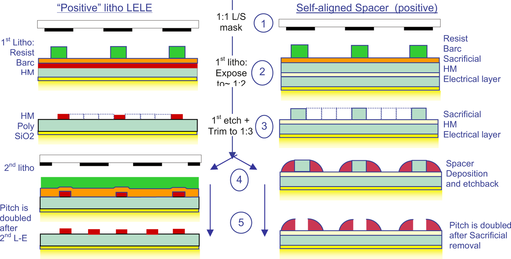
LELE & SOAP Patterning / SPIE
SADP is a very different way of doing things, but the end result is the same. The first step is doing a lithography/etch of dummy patterns that become the actual lines that are intended to be etched on the final pattern. Once this is done, a hard mask or similar material is deposited over the dummy patterns. After this, the hard mask is etched to expose the sidewalls that line the dummy patterns. Once all of this is completed, the dummy pattern is developed away and the exposed oxide is etched as usual. The result is that the lines are twice as close as before, and only one lithography pass was needed.
Unlike LELE and LFLE, there’s no need to be concerned about alignment because after the dummy pattern is set up, there’s no second exposure. This may be the reason why Intel's 22nm FinFET uses this process. Because the sidewall spacers are often created with hard mask materials, the resulting lines are also cleaner. This fact will become important, especially when discussing EUV and similar next generation lithography techniques.
While these techniques may sound like the perfect way to increase resolution, ultimately multiple patterning becomes increasingly expensive and difficult, especially because even a small misalignment between the two patterns can result in a wasted wafer. Multiple patterning also causes design restrictions that wouldn't occur with a true resolution increase in the lithography process because certain patterns become impossible with even order or odd order patterning processes.
Computational Lithography

Phase Shifting Mask / Stanley H. Chan
While we’re still talking about (relatively) low hanging fruit, I want to cover two other methods that are used to enhance resolution. The first is phase shifting masks. Rather than focusing upon wafer-level changes, this improves the reticle/mask itself. In short, this exploits the wave nature of light. There are two types of phase-shifting masks, and the first is an alternating phase-shift mask. This alters the thickness of the mask in some regions, which induces a phase-shift on the light waves that pass through it. As a result, there is interference with light from unmodified regions, which means that higher contrast can be achieved between the exposed and unexposed regions. The other type is the attenuated phase-shift mask, which only lets small amounts of light pass through that can interfere with the light coming from transparent regions.

Source Notes: Intended pattern in blue, OPC-corrected in green, final pattern in red.
Optical Proximity Correction / LithoGuy
The second is optical proximity correction, or OPC. One of the imperfections in the lithography process that we haven’t talked about until now is that what is drawn on the photomask/reticle is not translated exactly on to the photoresist. In reality, line widths vary greatly depending upon how dense the pattern around the line is; lines don’t end where they do on the mask, and the ends of lines are much thicker than the middle. OPC compensates for all of these effects and computes the photomask needed to achieve a layout close to the intended design.
Review
Summarizing things again, there are multiple techniques used to increase resolution to fabricate smaller transistors. By using lower wavelengths of light, multiple patterning techniques, and computational lithography techniques like phase shifting masks and optical proximity correction, we’ve managed to make it all the way down to 22 nanometer feature sizes. With the launch of Intel's Core M, we’ve made another jump down to 14 nanometers using the same light source that we did at 90 nanometers.


77 Comments
View All Comments
DanNeely - Friday, October 10, 2014 - link
A lot of them can only make n-type or p-type transistors. While that's not a problem for power or RF transistors; to control energy consumption and heat production you need both types to do CMOS logic gates.JoshHo - Friday, October 10, 2014 - link
While GaAs is popular in MMIC applications, it normally isn't possible to implement CMOS logic with such transistors.Lux88 - Friday, October 10, 2014 - link
Thank you very much for the much needed and very well written and illustrated introduction!How long does it take in real life to make a wafer with chips (with or without the testing)? Does it take hours, days or weeks to get a finished wafer with chips from silicon crystal?
At the end you mention a rate of "100+ wafers per hour", but I understand it as "number of wafers we are working on in parallel" rather than "number of wafers from start to finish".
aicjofs - Friday, October 10, 2014 - link
Time depends on the device and fab. Weeks though. I'd guess the average for any given chip(fron latest greatest down to simple microcontrollers) 3-6 weeks in the fab, another couple for testing packaging.He was talking about replacing a single photo tool(scanner/stepper) that does 100 wafers per hour with ebeam. There can be 10-100 scanners in fab, and as you say working in parallel.
ABR - Friday, October 10, 2014 - link
Great article. Our society has poured vast resources into this area at multiple levels and achieved incredible results. I can't help but think that if we had been motivated to put this kind of engineering effort towards space projects we would not only be colonizing Mars by now, but mining asteroids and running orbital solar panels. Maybe we'll eventually come back to these things, with new powers bestowed by this "inner space" technology. Or maybe not.pepone1234 - Friday, October 10, 2014 - link
This article is amazing!! Thank you for writing this :DKhenglish - Friday, October 10, 2014 - link
You missed the biggest reason why SOI has gone out of fashion from microprocessors. Costs and fabrication are not a big deal. All you do is implant O2 deep into the wafer, then heat it to turn the implanted O2 into SiO2. This is 2 extra steps of 400 or so done when processing a wafer. No big deal.The problem is that there is no more transistor body connection to ground. This means that the body can build up charge like in flash memory. What it ends up doing is skewing the threshold voltage. When doing high voltage work with radio or power electronics with big transistors this is no big deal, but with microprocessors it is a significant. Even worse is this charge depends on the previous state of the transistor and how long it has been in that state, which is difficult to predict, and thus we have unpredictable performance swings with SOI.
JoshHo - Friday, October 10, 2014 - link
This is a PD-SOI issue that falls under history effects mentioned in the article. FD-SOI doesn't have history effects as the body doesn't inherently have mobile charge carriers, which must be generated by band-bending.Khenglish - Friday, October 10, 2014 - link
So if FD-SOI gets rid of body effects then why is SOI not common? I supposed you can't just implant O2 and anneal for FD-SOI? Is sanding the wafer and growing SiO2 what needs to be done?The article also mentions temperatures, but the heatsink is attached to the interconnect side of the CPU instead of the bulk side from my understanding so this should have no impact.
JoshHo - Saturday, October 11, 2014 - link
The biggest issue continues to be cost. While continuing to push bulk CMOS is more expensive in up-front cost, SOI has much higher fluid costs. There's also only one supplier of SOI wafers to my knowledge. (Soitec)