An Introduction to Semiconductor Physics, Technology, and Industry
by Joshua Ho on October 9, 2014 3:00 PM EST- Posted in
- Semiconductors
- CMOS
- Physics
- Industry
- Technology
Interconnects
Finally, it’s time to talk about what lies ahead. One thing we haven’t talked about yet are the pressing issues of the near future. For example, there are major issues looming with interconnect delay that haven’t been solved yet. As we discussed in BEOL processing, the current system of wiring these metal layers uses copper with a dielectric in between the wires with a tantalum/tantalum nitride cap to support the next layer. However, the smaller the wires get, the worse electron mobility becomes.
This is roughly analogous to the issues that we see in the front end of line, which saw decreasing drive current for the same reasons. Combined with the capacitance produced between wires, there is dramatically increasing RC time delay in the connections made between transistors that hurts performance due to lower peak clock speeds. Ultimately, progress can only be made on this end by using lower k dielectrics and lower resistance materials to drive down both resistance and unwanted capacitance in these circuits.
Next Generation Lithography
There’s still more to talk about though. While we’ve managed to stretch 193mm immersion lithography further than anyone ever imagined, 10 nanometers is likely to be the end of the road for 193nm. Here, the future is unclear. Realistically, it seems that there are only a few techniques that will be viable at the next level. These include extreme ultraviolet lithography (EUVL), nanoimprint lithography, and electron beam lithography. Let's go over each one to try and understand what challenges are coming and which option may be the best in the long run.
EUV
On the surface, EUV is a relatively straight progression of the current 193i deep-UV (DUV) technology and should deliver the significant jump needed to advance lithography beyond 10 nanometer feature sizes. While this seems easy enough, there are a large number of issues that crop up from such a short wavelength (~13nm) of light.
First, the EUV light source itself is no longer a laser in most cases. This means that the energy efficiency of the light source is extremely low compared to current 193nm excimer lasers, and as a result an enormous amount of energy has to be used to generate an incoherent light source that is then filtered to only produce EUV.
Second, EUV is strongly absorbed by almost all matter. This means that the lithography must take place in a vacuum, which rules out techniques such as immersion lithography to further resolution enhancements. By using a strong vacuum for lithography, the amount of wafers that can be processed per hour drops dramatically as vacuuum chucks can no longer be used to hold the wafer, and the electrostatic chucks used must be heated to a stable temperature with a sacrificial wafer. Also, keeping the wafer heating from the EUV exposure becomes a significant issue because the immersion fluid that once cooled the wafer cannot be used.
In addition, it's impossible to use transmissive lenses because of this same issue. As a result, mirrors must be used to focus and reflect the EUV light on to the target. There are potential issues with EUV damaging the mirrors in the optical system, and in order to reflect the EUV light all of the mirrors and the photomask have to be coated with multiple layers that use interference effects to maximize reflected light. This also means that even minor defects in a photomask can result in an unusable photomask, as seen in the photo below.
Buried Defect on EUV Mask Blank / Guiding light / CC BY SA
Unfortunately, these defects cannot be seen using an electron microscope. In order to see these defects, an EUV microscope must be used. Outside of these challenges, EUV itself intrinsically has multiple issues that reduce resolution in some unexpected ways. First, shot noise becomes a serious issue. What this means is that it's fundamentally impossible to completely control the number of photons that are released into the photoresist. This means that the lines drawn by an EUV can be unacceptably rough unless enough photons are used to ensure that shot noise is statistically insignificant, but this only increases the power requirements for EUV lithography. To make things worse, by increasing the amount of exposure to the photoresist the material can be damaged by the sheer intensity of the heating effect of EUV.
Finally, because EUV is so energetic, it is a form of ionizing radiation. This means that when EUV light is absorbed by a molecule, electrons can be liberated. Unfortunately, this adds yet another source of uncertainty and also decreases resolution because the generated photoelectrons move randomly through the photoresist. In effect, all of these issues reduce the true resolution of EUV to somewhere around the 15-19nm feature size for a single exposure. In order to even get to 10nm and below, double patterning is required to reach the resolution necessary.
In short, the resolution gain from current 193nm technology is relatively small compared with the enormous expense and new design challenges. Based on how many delays have occurred with the introduction of EUV lithography, it may mean that a radically new system is needed to fabricate even smaller ICs. That's where nanoimprint and e-beam lithography come in.
Nanoimprint Lithography
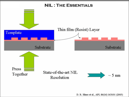
Nano Imprint / UMD
This type of lithography is incredibly simple. This method is simply using a thermoplastic polymer coated onto the substrate (such as a silicon wafer), and then a mold is pressed down on the wafer to print a pattern. Once this is done, a pattern transfer technique such as plasma etching is used to etch away the resist as necessary to expose the pattern on the wafer.
While this technique is simple and can easily be used as a next generation lithography tool, there are also a number of flaws involved with this process. If the imprinting isn't done in a vacuum, there is a high likelihood that the mold will have air bubbles that alter the pattern in unpredictable ways. In addition, the template is susceptible to wear and tear, which means that resolution is lost as the mold is repeatedly used in imprinting. The imprint mold must also take into account uneven depth of imprinting based on the density of the pattern used and potential stretching of the resist. Finally, making the template itself requires extremely precise lithography, which means that it's limited by current generation lithography techniques in resolution. This isn't a solution by itself, which means it can only be used in conjunction with other methods.
Electron Beam Lithography
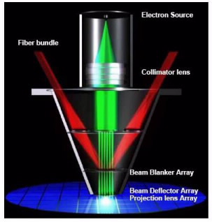
Electron Beam Lithography / SEMI
Just as we saw in the progression of microscopes, the early days were mostly focused on improving light microscopy with higher NA lenses and oil immersion, but today some of the highest resolution microscopes use electrons instead of photons. Similarly, electron beam lithography can generate some of the highest resolutions possible out of all the lithography techniques we've discussed in this article. This means that sub-10nm resolution is easily achieved. In fact, it's fully possible to do away with the resist and simply write the pattern directly on the silicon wafer, eliminating the resist as a potential bottleneck for resolution.
Unfortunately, this system is extremely slow. Rather than the 100+ wafers per hour of current photolithography techniques, electron beam lithography is often limited to less than ten wafers per hour. Using a single electron beam to write an entire 300mm wafer would take around 22 years. While thousands of beams can be simultaneously writing to the wafer to speed up the process, the electrons begin to affect the trajectory of other electrons in other beams. This requires complex modeling to compensate for such effects.
As with EUV lithography, shot noise becomes a significant issue despite a much easier ability to control the dose. This is because even small variations in the number of electrons can significantly effect the roughness of the lines drawn by the electron beam. There is also a strong need to choose a balanced energy for the electron, as excessively energetic electrons can cause significant secondary electron generation, but too little energy means the electrons are easily scattered. Both reduce resolution and can result in unacceptable defects for smaller process nodes.


77 Comments
View All Comments
Khenglish - Thursday, October 9, 2014 - link
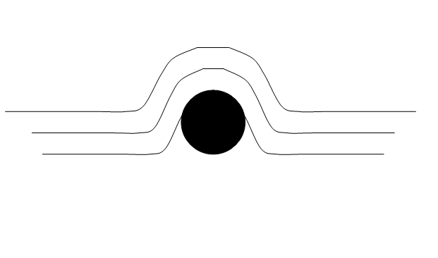
Curving the wafer actually has major impacts on electronic operation. For example wafer bending is currently done by implanting Germanium into the wafer for PFETs. Because Ge is larger than Si, this causes the wafer to bend. This bend increases hole mobility making PFETs more conductive and faster, but slows down NFETs, thus manufacturers implant Ge only at PFET locations. This processes of bending the wafer by implanting Ge is strained silicon, and 1st started showing up around the 130nm era. It is done because for similarly sized transistors, NFETs are around 2.7x more conductive than PFETs without strained silicon.EMM81 - Monday, October 13, 2014 - link
There is definitely no curving or any wafer. Ge is used to strain the silicon crystal latice. Ge is in the same group on the periodic table and forms the same diamond cubic crystal structure. Grading a fraction of Ge (larger atoms longer bond lengths) into the Silicon latice the silicon bonds effectively get stretched (see image in article). This has a physical effect on the mobility of electrons and holes. Curving a wafer is a non-starter as NONE of the standard processing techniques would work...wafers have to be not only flat but ultra flat for litho optics, dry etch, wet etch spinners, ion implanters...hlovatt - Thursday, October 9, 2014 - link
Great article. More please!witeken - Thursday, October 9, 2014 - link
Awesome, thanks for the great article.However, 22nm doesn't have a single feature size of 22nm. It's just a name, and so are 28nm, 20nm, 16nm, 14nm,...
For example, the fins of 22nm are 8nm while the gate pitch is 90nm. (http://images.anandtech.com/doci/8367/14nmFeatureS...
Khenglish - Thursday, October 9, 2014 - link
When you hear 22nm, 32nm, 16nm, etc the number you are hearing is the smallest feature size that can be imprinted via lithography. This is not necessarily the smallest feature size than can be implemented on the process.EMM81 - Monday, October 13, 2014 - link
This is not true. Node size was loosely defined as the half pitch of either the poly-silicon gate or the tightest metal pitch. The node size designation however, has not followed the minimum half pitch for many technologies, from any of the fabs. Node size is now a purely marketing term. If a fab were to implement HKMG, strained silicon...these things would not necessarily have any effect on the dimensions of transistors but they would result in improvements to the chip performance. Density is only 1 component that plays into node designation these days and even then density of the transistors is being tightened by some fabs while leaving the density of the upper layers unchanged.Khenglish - Wednesday, October 15, 2014 - link
Again just because lithographic features can be made a certain size does not mean you make everything that size. Maybe there is just one minor feature that is really that size. I'm saying that process size is the minimum size that can cut by the ebeam into a lithography mask and transferred if the design calls for it. This is why when looking at a processor that the feature size is so hard to quantify. Just one feature at whatever they advertise can let them call it that number. Yes feature size doesn't need to have anything to do with density or performance and is mostly a marketing thing.Keisari - Thursday, October 9, 2014 - link
A very necessary article. Great initiative!martixy - Thursday, October 9, 2014 - link
There's probably something to be said about breezing through this(of my own free will moreover), while having such a hard time with the exact same material from the textbook.Go figure.
Murloc - Thursday, October 9, 2014 - link
It's meant to be intuitive and summarized in a limited amount of space. That's why it's easy to read. It has way less depth than a textbook.