Samsung SSD 850 Pro (128GB, 256GB & 1TB) Review: Enter the 3D Era
by Kristian Vättö on July 1, 2014 10:00 AM EST3D NAND: Hitting The Reset Button on Scaling
Now that we understand how 3D NAND works, it is time to see what it is all about. As we now know, the problem with 2D NAND is the shrinking cell size and the proximity of the cells, which results in degraded reliability and endurance. Basically, 3D NAND must solve these two issues but it must also remain scalable to be economical. So how does it do that? This is where the third dimension comes into play.
The cost of a semiconductor is proportional to the die size. If you shrink the die, you effectively get more dies from a single wafer, resulting in a lower cost per die. Alternatively you can add more functionality (i.e. transistors) to each die. In the case of NAND, that means you can build a higher capacity die while keeping the die size the same, which gives more gigabits per wafer and thus reducing cost. If you cannot shrink the die, then you have just hit a dead-end because the cost will not scale. That is what has happened with 2D NAND because the shrinks on X and Y axes have run out of gas.
What 3D NAND does is add a Z-axis to the game. Because it stacks cells vertically, it is no longer as dependent on the X and Y axes since the die size can be reduced by adding more layers. As a result, Samsung's V-NAND takes a more relaxed position on the X and Y axes by going back to a 40nm process node, which increases the cell size and leaves more room between individual cells, eliminating the major issues 2D NAND has. The high amount of layers compensates for the much larger process node, resulting in a die that is the same size and capacity as the state of the art 2D NAND dies but without the caveats.
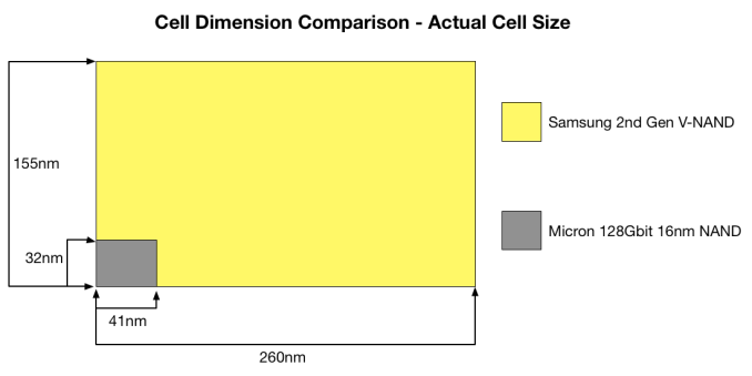
The above graph gives some guidance as to how big each cell in V-NAND really is. On the next page, I will go through the method of how cell size is really calculated and how V-NAND compares with Micron’s 16nm NAND but the above gives a good picture of the benefit that 3D NAND has. Obviously, when each cell is larger and the distance between individual cells is higher, there are more electrons to play with (i.e. more room for voltage state changes) and the cell to cell interference decreases substantially. Those two are the main reasons why V-NAND is capable of achieving up to ten times the endurance of 2D NAND.
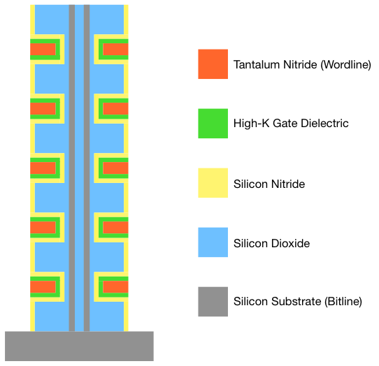
Moreover, scaling in vertical dimension does not have the same limitations as scaling in the X and Y axes do. Because the cost of a semiconductor is still mostly determined by the die area and not by the height, there is no need to cram cells very close to each other. As a result, there is very little interference between the cells even in the vertical direction. Also, the usage of high-K dielectrics means that the control gate does not have to wrap around the charge trap. The result is that there is a hefty barrier of silicon dioxide (which is an insulator) between each cell, which is far more insulating than the rather thin ONO layer in 2D NAND. Unfortunately, I do not know what is the exact distance between each cell in the vertical dimension but I think it is safe to assume that it is noticeably more than the ~20nm in 2D NAND since there is no need for aggressive vertical scaling.
As for how far Samsung believes their V-NAND can scale, their roadmap shows a 1Tbit die planned for 2017. That is very aggressive because it essentially implies that the die capacity will double every year (256Gbit next year, 512Gbit in 2016 and finally 1Tbit in 2017). The most interesting part is that Samsung is confident that they can do this simply by increasing the layer count, meaning that the process node will stay at 40nm.


160 Comments
View All Comments
Squuiid - Saturday, March 14, 2015 - link
Plus, the MX100 reliability is horrible. Just google MX100 BSOD, disappearing drive.I have 2x MX100 512GB SSDs and I recommend you don't buy one, no matter how cheap they are.
nightauthor - Tuesday, July 1, 2014 - link
For business purposes, I would rather pay twice as much and get a 10 year warranty vs the 3 year supplied by Crucial. Though, for my daily, I would probably go with the Crucial.TheWrongChristian - Wednesday, July 2, 2014 - link
No current SATA drives push low queue depth random IOs to the point of saturating SATA II, let alone SATA III.At high queue depths, perhaps. But then, that is not a typical workload for most users, desktop or server.
Plus, it's a new drive, prices will come down.
jwcalla - Monday, June 30, 2014 - link
Unless they're doing 5% OP the capacities are kinda... off.melgross - Monday, June 30, 2014 - link
I think there's a slight misunderstanding of manufacturing cost. While the die size may be the same, or even smaller than a competing technology, the 32 level chip does cost more to make per area. There are more masks, more layers, more etching and washing cycles, and more chance of defects.Right now, I do see why the cost is higher. I can on,y assume that as this technology progresses, that cost will drop per area. But it will always remain higher than an SLC, MLC or TLC chip.
So there is a balance here.
Kristian Vättö - Tuesday, July 1, 2014 - link
You are correct. I did mention yield and equipment cost in the final paragraph but I figured I won't go into detail about masks and etching since those would have required an in-depth explanation of how NAND is manufactured :)R0H1T - Tuesday, July 1, 2014 - link
It would be great if Anand or you do a writeup on 3d NAND & deal with the specific pros & cons of it as compared to traditional 2d NAND & if possible include something related to manufacturing processes of these & how they're different OR more/less expensive, certainly as in case of V-NAND?MrSpadge - Tuesday, July 1, 2014 - link
You wouldn't need too much detail - just saying that the number of process steps increases by probably around an order of magnitude should make this pretty clear.frenchy_2001 - Tuesday, July 1, 2014 - link
It is probably more than that, as Samsung is currently manufacturing 32 layers of cells. Each layer requires multiple operations (deposit, etching, washing...). Their biggest advantage comes from regressing to 40nm: at that technology, each operation is *MUCH* cheaper than the equivalent one at 1X pitch (15~19nm).So, total cost is an unknown, but should be very competitive, after recovering the initial R&D investment.
Spatty - Tuesday, July 1, 2014 - link
And not to mention 3D NAND is still basically bleeding edge. It's still in the stages of where a new DDR generation arrives, much higher costs then current gen.