Samsung SSD 850 Pro (128GB, 256GB & 1TB) Review: Enter the 3D Era
by Kristian Vättö on July 1, 2014 10:00 AM EST3D NAND: How It Works
To understand how 3D NAND helps to keep Moore's Law in action, we first need to go in-depth with the structure. Before we begin, there are a couple of disclaimers I want to get out. First of all, every manufacturer has a different 3D NAND structure, so to avoid information overflow and confusion, I will only talk about Samsung's structure for now. When other manufacturers are ready with their 3D NAND products, I will provide a similar analysis of their structure. Secondly, there is not much detailed information about Samsung's 3D NAND, or V-NAND as they call it, so I am mostly basing my analysis on The Memory Guy's blog post (also known as Jim Handy, a respected semiconductor analyst).

What you are seeing above is a 5-layer 3D NAND string based on Samsung's TCAT (Terabit Cell Array Transistor) structure. It consists of a total of ten cells and similar to 2D NAND each cell is capable of holding one, two or three bits of data depending on whether the NAND is SLC, MLC or TLC. Samsung's current (i.e. second) generation V-NAND has 32 layers, meaning that it is simply a taller tower but to keep the graph easily readable I decreased the number of layers to five.
There is one fundamental difference between Samsung's V-NAND. With 2D NAND, the charge was stored in a conductive floating gate but as you can see in the graph above, there is not one in Samsung's V-NAND. Instead Samsung uses a design called Charge Trap Flash (CTF), which means that the charge is stored in an insulator, which is silicon nitride in this case.
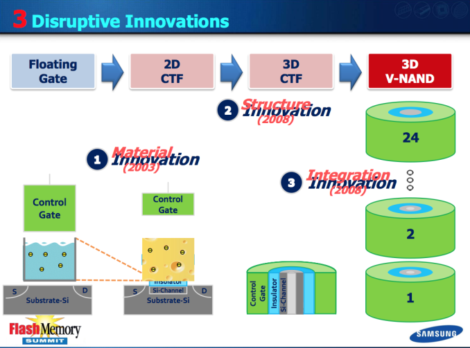
Some of you might remember this rather hilarious slide we used in our V-NAND announcement article and I now have an explanation as to why Samsung used cheese in in (yes, it indeed is cheese). A traditional floating gate works pretty much like a bucket of water. As long as there is not a hole in the bucket, the water stays there without an issue. However, if you get even a tiny hole in the bucket, all the water will sooner than later escape through that hole. It is the same with a floating gate because if there is a hole in the insulating material around it (Inter Poly Dielectric and tunnel oxide), all the electrons in the floating gate will escape through that as the floating gate is conductive and the electrons can move freely. As I mentioned on the previous page, this is exactly what happens when NAND is cycled and wears out because the stress caused by the programming operation causes the insulators to lose their insulating characteristics.
With Charge Trap Flash that does not happen because the electrons reside in an insulator. Samsung compared the bucket of water idea to cheese, meaning that if there is a hole the cheese will not just pour out from it like water would.
As a result, Charge Trap Flash increases endurance as it is not as vulnerable to wear out. I am also told that CTF does not require as high programming voltages as floating gates do (up to 20V), which reduces the stess on the insulators. I wonder if this is simply because the insulators do not have to be that thick anymore (a miminum of 7nm for tunnel oxide and 12nm for ONO) because the charge trap is not as dependent on the surrounding insulators as floating gate is. The reason why such a high voltage is needed for 2D NAND programming is the thickness of the tunnel oxide because otherwise the electrons cannot tunnel through (remember, the electrons are shot through an insulator). On the other hand, the tunnel oxide cannot be made any thinner than 7nm or otherwise data retention takes a massive hit (NAND is really an engineers dream, isn't it? Touch one thing and you break another).
Another interesting tidbit regarding Samsung’s V-NAND is the usage of a high-K dielectrics. IMFT did a similar switch when they moved to 20nm node but all the other manufacturers, as far as I know, have stayed with an inter poly dielectric (IPD) design. I went into detail about high-K dielectrics in our Crucial MX100 review but I will provide a quick summary here. Basically, a high-K dielectric is a material with a high dielectric constant, which is quite surprisingly known as K. The benefit of a high-K dielectric over a normal dielectric (like oxide-nitride-oxide i.e. ONO in NAND) is that it provides a higher capacitance between the word and bitlines. Similar to 2D NAND, the capacitance between the control gate and the floating gate, or charge trap in the case of V-NAND, is still the key factor for operation. The usage of high-K dielectrics gives Samsung a bit more headroom in terms of vertical scaling as layers can be stacked closer to each other and it also improves endurance as high-K dielectrics have less leakage compared to normal dielectrics.
Otherwise the basics of V-NAND are very similar to 2D NAND. To program a cell, the bitline is grounded (i.e. held at 0V) while a high voltage is placed on the wordline. That makes the electrons that are floating in the bitline to tunnel through the silicon dioxide to the charge trap a.k.a. silicon nitride.

I made a very simple graph of V-NAND programming, which should help you to understand the process. The elements are the same as in the tower graph with the difference that it is just one layer and I cut the tower in half to fit it on the page. The purple balls are electrons.
Reading from V-NAND works exactly the same as with 2D NAND. The wordline of the cell-to-be-read is held at 0V while different voltages are applied on the bitline. Once the correct voltage is found, the cell will conduct and the sense amp will read the data depending on what the voltage was (the voltage determines the voltage state, i.e. what the value is).


160 Comments
View All Comments
Krakadoom - Saturday, September 27, 2014 - link
I bought the 850 Pro 500 GB version. The transfer speeds are around (and just under) 400 MB/s and the IOPS are always around 55-60k. Not impressed - considering returning it just due to the huge gap between the rated specs and actual performance. (Of course Samsung Magician over-reports the transfer speed by quite a large margin).stealth_lee - Wednesday, October 1, 2014 - link
Someone just tipped me that V-NAND in Samsung 850 Pro is actually TLC not MLC.The first reason is the 86Gbit/die number is odd, if 850 Pro uses a TLC 128Gbit/die and emulates it to MLC then it would be 86Gbit/die, the numbers fit well.
The second reason is Chipworks confirmed it in the die shots:
http://bit.ly/YTVm9Z
http://bit.ly/1uByKcm
I'm just the messenger here, I'm not expert.
So...I was wodering is it possible to hack Samsung 850 Pro to get extra storage space in TLC?
wcatlan - Saturday, October 25, 2014 - link
Why isn't the lack of power loss protection a showstopper for any of these drives? I love the speed and reliability benefits under normal operation, but how can anyone get excited about a drive that can get corrupted in an instant due to power loss or computer freeze, where a hard shutdown is required? Seems that these drives are more prone to massive data issues much more than HDDs under the same power fault conditions. I keep looking for a good answer, but it seems smart people are willing to look past this seemingly fatal Achilles heal. Not sure what I might be missing. Any thoughts?futurefilm - Monday, December 1, 2014 - link
Today, Cyber Monday deals on Amazon, the 850 Pro 256 is going for $150. The 128 for $100. Get it now while it's hot.saagar - Thursday, January 22, 2015 - link
Dear Kristian Vättö,Fantastic review of the drives and the technology behind it. This is what readers like me expect to see on Anandtech. Thanks for breaking it down. Keep up the good work!
gsuburban - Wednesday, April 8, 2015 - link
As of April 8, 2015, the 850 Pro 256GB SSD can be had for about $144 if you look hard enough.rockfella79 - Saturday, June 27, 2015 - link
I love my 850 Pro 128 GB SSD :)KDT - Thursday, March 24, 2016 - link
Please update the endurance to 300TBW for 1TB model. This was my basis for buying this SSD. This is 2nd to Crucial MX200 (320TBW on 1TB model) in terms of endurance - for client/consumer SSDs.BimmerInd - Sunday, June 26, 2016 - link
Samsung is using 40nm over Micron's 16nm. Doing the math implies that for every 2.5 16nm Micron nodes in planar section, Samsung only does 1 40nm node. If we scale vertically to 32 layers, then Micron (or others for that matter) still do only 2.5 nodes for every 32 nodes of Samsung. Which means for every 16nm node, Samsung provides 12.8 nodes. Meaning the density scaling factor for every 32 layer increments is a multiple of 12.8. Assuming the current die size for 32 layers to be 128Gbit, then the density advantage for 256Gbit is 12.8x2 times, 512Gbit is 12.8x4 times and for 1Tbit in 2017 should be 12.8x8 times for 256 layers of nodes stacked on top of each other. So the density advantage is approximately 102.4% (theoretically). Samsung can theoretically produce a 1Tbit die at a cost advantage/space advantage of nearly 100 times compared to planar and manufacturers. It is almost like you are able to earn 100 times the profit for the same die provided the cost per bit is scaled along without passing on the price advantage to the end users until other players enter 3D market.The same is the case with Intel's 3D Cross Point Technology. They are having a new tech in their hands that is faster than NAND and closer to DRAM. So they are also planning to price it exactly between NAND and DRAM. We are already paying high costs to shift from platters to NAND and are going to pay even more to make a shift from NAND to 3D xPoint. I just wish I can jump a few years to the future, grab a high capacity NAND/xPoint drive for cheap and come back to the present and use it. Sigh !
BimmerInd - Sunday, June 26, 2016 - link
By the way this is just a rough calculation and is not to be taken literally.