Intel 2014 Enthusiast Processors: Haswell-E To Feature 8 Cores, X99, DDR4
by Ian Cutress on March 19, 2014 8:00 PM EST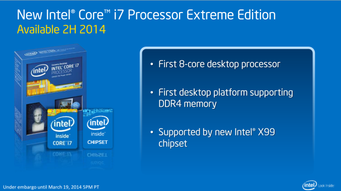
The second of Intel’s enthusiast-based announcements after the unlocked Iris Pro coming to Broadwell is one regarding Intel’s new high performance platform. Currently we sit with socket LGA 2011 featuring Sandy Bridge-E and Ivy Bridge-E CPUs on top of the X79 chipset using DDR3 memory. Intel are confirming today that the next stage in that process will be Haswell-E, supported by the new X99 chipset and flanked with DDR4 memory.
The new processor line up will have an 8-core CPU at the top end, which Intel is calling their first ‘8-core desktop processor’ (strictly speaking Avoton is a server part). Given that the Xeon line of Ivy Bridge-E CPUs can hit 10, 12 and 15-core counts as we have reviewed, it should have been possible for Intel to consider these core counts for the enthusiast platform. However Intel has no competition in this area to innovate, so while core counts may rise on the Xeon side of the equation, for the consumer line we will have to wait longer for anything more than 8 cores.
The shift to DDR4 memory has been expected for a number of quarters. Speculation initially revolved around DDR4 coming earlier than Haswell-E, but we have to consider the enterprise market on this one. As many Ivy Bridge-E users have lamented, staying with the X79 platform has put consumers on the back foot when it comes to connectivity compared to the 8-series platform. X79 is down on USB 3.0 ports, SATA 6 Gbps ports and no mention of Flex-IO. So with X99 and DDR4, given that we expect to keep this platform for at least Haswell-E and Broadwell-E (potentially 2.5 to 3 years), it comes in now in preparation for the future platforms. We have seen DDR4 modules being tested at various trade shows, and I would imagine that most of the major memory partners (especially the enthusiast lines) are currently preparing kits.
The X99 platform is almost a complete unknown at this point. Given that Intel state that Haswell-E is planned for 2H 2014, we have had no information. In order to remain as the top end platform in the chipset sense (and not fall behind like X79), I would imagine X99 to take many cues from Z87 and even from the 9-series motherboards we have seen at CeBIT. This should mean a full complement of SATA 6 Gbps ports and USB 3.0 ports, with support for M.2, although we have no confirmation. Similarly while I would expect Flex IO to be present, allowing manufacturers to vary the number of PCIe 2.0 lanes from the chipset in exchange for SATA 6 Gbps ports and USB 3.0 ports, we also have no confirmation. In the past there have been X79 products with SAS support, although these were extra parts of the chipset that were not part of the validation process. It would be interesting to see if any of that functionality makes its way in. Flex IO seems like the future of flexible chipset design, and it would be interesting to see if Intel thinks this way as well.
As mentioned, and in the slide, Haswell-E is due in the second half of 2014. We unfortunately have no extra information on that date, but it confirms 2014 rather than 2015 which had been speculated.


45 Comments
View All Comments
iwod - Thursday, March 20, 2014 - link
Ok I am confused ( I haven't been following Desktop CPU for a long time )Did Intel ever had a LGA 2011 i7 Desktop Chip? Because i couldn't not find any on Intel Ark website. They were all 1155. Even the 3rd Generation.
If yes, then why is this 8 Core new to Desktop. Since on server side there are already 8 Core IvyBridge E5 v2 based on Socket 2011 as well.
Broadwell is delayed on Desktop. Mobile coming first. So the 2015 year of Skylake we will see a Desktop Broadwell?
Um this is all a bit strange, at least the way things work are no longer predictable with the Tick Tock timeframe.
f0d - Thursday, March 20, 2014 - link
"Did Intel ever had a LGA 2011 i7 Desktop Chip?" yes there was many 3820 3930k 3960x 4820k 4930k 4960x"If yes, then why is this 8 Core new to Desktop" because they were all 4 and 6 core cpus
BMNify - Thursday, March 20, 2014 - link
"The shift to DDR4 memory has been expected for a number of quarters. "actually its clear that while DDR4 will give you a potential 1.5x to 2x better ram data throughput, it all seems far to little far to late now, i still cant see the masses of industrial cloud installations etc wanting to pay for the limited benefit when its clear for a long time now that ratified HMC (hybrid memory cube) at lower power and 17x's the data throughput are also almost here in bulk manufacture, it just takes the orders to the foundries to make it happen...
""More than 100 developer and adopter members of the hybrid memory cube consortium (HMCC) this week announced is has reached consensus for the global standard that will deliver a much-anticipated, disruptive memory computing solution. Developed in only 17 months"
"More than 100 leading technology companies from Asia, Japan, Europe and the U.S. have joined the effort, including Altera, ARM, Cray, Fujitsu, GlobalFoundries, HP, IBM, Marvell, Micron Technology, National Instruments, Open-Silicon, Samsung, SK Hynix, ST Microelectronics, Teradyne and Xilinx. Continued collaborations within the consortium could ultimately facilitate new uses in HPC, networking, energy, wireless communications, transportation, security and other semiconductor applications."
jasonelmore - Thursday, March 20, 2014 - link
all those companies dont matter unless intel is on the list. they have to bake support into their platforms, or you will see hardly any adoption given ARM's market share in the server marketBMNify - Thursday, March 20, 2014 - link
you seem unaware that in fact Intel where one of the original developers of HMC at the fall Intel Developer Forum in September 2011.customers like Intel and AMD are not consortium members, it is generally thought that they opted not to be involved in the open standard in order to develop their own way of using the technology. Intel demonstrated a prototype HMC device during the fall Intel Developer Forum in September 2011, deeming it the fastest and most efficient DRAM ever built..."
http://www.i-micronews.com/upload/image/PG/compare...
BMNify - Thursday, March 20, 2014 - link
http://blogs.intel.com/intellabs/2011/09/15/hmc/Reinventing DRAM with the Hybrid Memory Cube
By Bryan Casper on September 15, 2011
"Today, Intel CTO Justin Rattner is demonstrating the Hybrid Memory Cube, the fastest and most efficient Dynamic Random Access Memory (DRAM) ever built.
I want to give you some background on how and why we collaborated with Micron on this new memory technology. One of my research passions is helping to design computers to be faster and more energy efficient.
A portion of my creative energy over my career has been to improve the interconnect within computer systems so that communication between the microprocessor, DRAM, storage and peripherals is faster and lower power with each successive generation. In other words, I’m an I/O guy.
One of the biggest impediments to scaling the performance of servers and data centers is the available bandwidth to memory and the associated cost. As the number of individual processing units (“cores”) on a microprocessor increases, the need to feed the cores with more memory data expands proportionally.
Legacy DDR-style of DRAM main memory isn’t going to cut it for much of the future high-end systems. Being an I/O researcher, my initial efforts to solve the memory bandwidth problem were focused exclusively on the I/O to improve the circuits, connectors and wires that help to form the connection between the microprocessor and memory...."
iwod - Thursday, March 20, 2014 - link
Well iGPU is heavily bottlenecked by Memory Bandwidth as well. So why Isn't Intel bringing this to Market instead?BMNify - Thursday, March 20, 2014 - link
good question, perhaps anand can ask themBMNify - Thursday, March 20, 2014 - link
you also seem unaware as regards "they have to bake support into their platforms, or you will see hardly any adoption given ARM's market share in the server market" that in fact many of the best server kit is in fact now using ARM SoC IP NoC (Network On a Chip), CoreLink CCN-508 that can deliver up to 1.6 terabits of sustained usable system bandwidth per second with a peak bandwidth of 2 terabits per second (256 GigaBytes/s)its also interesting to note that with the defined "short-reach (SR) and ultra short-reach (USR) interconnection across physical layers (PHYs) for applications requiring tightly coupled or close-proximity memory support " and the generic current CoreLink CCN-508 that can deliver up to 1.6 terabits of sustained usable system bandwidth per second with a peak bandwidth of 2 terabits per second (256 GigaBytes/s) at processor speeds scaling all the way up to 32 processor cores total..... at least on paper
Intel's Knights Landing Xeon Phi due in 2015 with its antiquated QPI interconnect and its expected ultra short-reach (USR) interconnection only up to 500MB/s data throughput seems a little/lot short on real data throughput by then, Intel seem to need to go to Wide IO/HMC and a far better ultra short-reach interconnect ASAP it seems....
Khato - Thursday, March 20, 2014 - link
So many errors I have to wonder if it's all intentional?So, what are some examples of these 'best server kit' that use ARM's CoreLink CCN-508? Which was only announced late last year by the way, hence why there are no products using it yet. Second, it's an on-chip interconnect and hence that peak bandwidth isn't anything special.
As for Knight's Landing, QPI is an external interconnect use for communication between packages through common PCB traces and capable of over 25 GB/s. And you know that Knight's Corner already has a peak memory bandwidth of 352 GB/s, right? Care to take a guess at the sustained bandwidth its on-chip interconnect is capable of? I'd imagine not since you want to pretend that ARM's CCN-508 is something awesome and revolutionary.