Imagination's PowerVR Rogue Architecture Explored
by Ryan Smith on February 24, 2014 3:00 AM EST- Posted in
- GPUs
- Imagination Technologies
- PowerVR
- PowerVR Series6
- SoCs
When it comes to our coverage of SoCs, one aspect we’ve been trying to improve on for some time now is our coverage and understanding of the GPU portion of those SoCs. In the PC space we’re fortunate that there are just three major players – Intel, NVIDIA, and AMD – and that all three of them have over the years learned how to become very open and forthcoming about their GPU architectures. As a result we’ve had a level of access that has allowed us to better understand PC GPUs in a way that in earlier times simply wasn’t possible.
In the SoC space however we haven’t been so fortunate. Our understanding of most SoC GPU architectures has not been nearly as deep due to the fact that SoC GPU designers have been less willing to come forward with public details about their architectures and how those architectures have evolved over the years. And this has been for what’s arguably a good reason – unlike the PC GPU space, where only 2 of the 3 players compete in either the iGPU or dGPU markets, in the SoC GPU space there are no fewer than 7 players, all of whom are competing in one manner or another: NVIDIA, Imagination Technologies, Intel, ARM, Qualcomm, Broadcom, and Vivante.
Some of these players use their designs internally while others license out their designs as IP for inclusion in 3rd party SoCs, but all these players are in a much more competitive market that is in a younger place in its life. All the while SoC GPU development still happens at a relatively quick pace (by GPU standards), leading to similarly quick turnarounds between GPU generations as GPU complexity has not yet stretched out development to a 3-4 year process. As a result of SoC GPUs still being a young and highly competitive market, it’s a foregone conclusion that there is still a period of consolidation ahead of us – not unlike what has happened to SoC integrators such as TI – which provides all the more reason for SoC GPU players to be conservative about providing public details about their architectures.
With that said, over the years we have made some progress in getting access to the technical details, due in large part to the existing openness policies of NVIDIA and Intel. Nevertheless, as two of the smaller players in the mobile GPU space this still leaves us with few details on the architectures behind the majority of SoC GPUs. We still want more.
This brings us to today. In what should prove to be an extremely eventful and important day for our coverage and understanding of SoC GPUs, we’d like to welcome Imagination Technologies to the “open architecture” table. Imagination chosen to share more details about the inner workings of their Rogue Series 6 and Series 6XT architectures, thereby giving us our first in-depth look at the architecture that’s powering a number of high-end products (not the least of which is all of Apple’s current-gen products) and descended from some of the most widely used SoC GPU designs of all time.

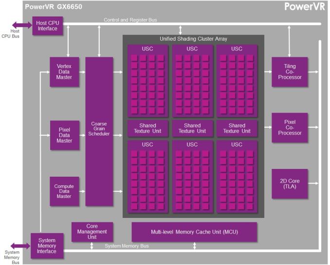
Now Imagination is not going to be sharing everything with us today. The bulk of the details Imagination is making available relate to their Unified Shading Cluster (USC) shading block, the heart of the Series 6/6XT GPUs. They aren’t discussing other aspects of their designs such as their geometry processors, cache structure, or Tile Based Deferred Rendering system – the company’s secret sauce and most potent weapon for SoC efficiency – but hopefully one day we’ll get there. In the meantime we will have our hands full just taking our first look at the Series 6/6XT USCs.
Finally, before we begin we’d like to thank Imagination for giving us this opportunity to evaluate their architecture in such great detail. We’ve been pushing for this for quite some time, so we’re pleased that this is coming to pass.
Imagination is publishing a pair of blogs and pseudo whitepapers on their website today: Graphics cores: trying to compare apples to apples, and PowerVR GX6650: redefining performance in mobile with 192 cores. Along with this they have also been answering many of our deepest technical questions, so we should have a good handle on the Rogue USC. So with that in mind, let’s dive in.


95 Comments
View All Comments
vladz - Monday, February 24, 2014 - link
So what does flexible hardware or flexible rendering mean exactly?Ryan Smith - Monday, February 24, 2014 - link
Flexible hardware in the context I used it would mean programmable.TMUs aren't flexible. They fetch texels, apply filtering, and that's it.
Shaders are flexible. They accept threads of instructions and the result on a pixel/vertex will be whatever the program dictates, as opposed to a fixed outcome.
ifrit39 - Monday, February 24, 2014 - link
I believe your math is off on the last table. GTX 650 would produce 230.4 GFLOPS @ 300MHz, not 330.4.Its interesting to me that these mobile designs are so close to full desktop performance (albeit with the low 300MHz clock). But memory bandwidth, power, and clocks will always hold these SoCs back in the real world.
Thanks for the great article, as always.
hoboville - Monday, February 24, 2014 - link
I love these kinds of articles, simply because of the explanations of how various hardware and underlying systems work. Probably the best part of Anandtech reviews.Laststop311 - Tuesday, February 25, 2014 - link
Gotta give imagination tech some credit. They have the highest performing gpu's in the soc market. Very flexible too, they make a 2 core cluster , 3 core, 4 core and 6 core. If only we could have the best cpu performance (qualcomm snapdragon krait cpu's) mixed with the best gpu (powervr 6xt 6 core version) on the same soc. Tho nvidia dual core denver design that throws away all the extra cores and devotes more die space to 2 higher performing more complex cores might take the cpu crown since there arent many workloads on a phone that needs more then 2 threads going.nosirrah123 - Tuesday, February 25, 2014 - link
Wow, this is an amazingly written article, good work!patrickjchase - Tuesday, February 25, 2014 - link
Are you sure that Rogue is superscalar rather than VLIW?Briefly the difference between the two comes down to when independent instructions (ones that can execute in parallel) are identified. In a VLIW it happens at compile time, while in a superscalar design it happens at runtime. It would actually surprise me if Rogue does runtime dependency analysis for such a wide backend - If I had to bet I'd say "VLIW".
D16700605001 - Wednesday, February 26, 2014 - link
is there a similar article comparing Nvidia to AMD? I've seen block diagrams of Nvidia chips on their web site but haven't found any for AMD. Even if I did, an article like this one would be better than me trying to make inferences and decode the vendor spin. I want to buy a compute engine and I keep getting the impression AMDs offering is better but would like to be convinced from a technical discussion rather than stats about game performance and unpacking textures.Bawl - Saturday, March 1, 2014 - link
Great article. Thank you so much. PowerVR has so much power inside, I can only think their power are underutilized because of the others GPUs.MrSpadge - Saturday, March 1, 2014 - link
I wonder how many instructions they can dispatch per clock. That's a significant factor when discussing how to feed up to 7 execution units. Actually I'd be surprised if it's more than 2, maybe 3 under special circumstances.. which would make me wonder how they're feeding 4 FP16 ALUs. But then I also wonder if these are truly 4 independebt units.. I guess not.