The NVIDIA GeForce GTX 750 Ti and GTX 750 Review: Maxwell Makes Its Move
by Ryan Smith & Ganesh T S on February 18, 2014 9:00 AM ESTMaxwell: Designed For Energy Efficiency
While Maxwell doesn’t come with a significant overhaul of its high level feature set, the same cannot be said for the low level design of Maxwell. In fact the consistency at a high level betrays just how much work NVIDIA has done under the hood in order to improve their efficiency for Maxwell. Maxwell isn’t a complete overhaul of NVIDIA’s designs, nor is it even as aggressive as Kepler was when it eliminated Fermi’s hot clocks in favor of a wider design, but it has a number of changes that are important to understanding the architecture and more importantly understanding how NVIDIA is achieving their efficiency goals.
Broadly speaking, with Maxwell NVIDIA is almost solely focused on improving energy efficiency and performance per watt. This extends directly from NVIDIA’s mobile first design strategy for Maxwell, where the company needs to maximize energy efficiency in order to compete and win within the mobile space. If NVIDIA can bring down their energy consumption, then due to the power limiting factor we mentioned earlier they can use that recovered power overhead to further improve their performance. This again being especially noticeable in SoC-class products and discrete mobile due to the low power budgets these platforms provide.
To a lesser extent NVIDIA is also focused on space efficiency. GPU production costs and space efficiency go hand-in-hand, so there’s an interest in improving the density of their designs with Maxwell. This is especially the case when the earlier power savings allow for a wider GPU with a larger number of functional units within the same power envelope. Denser designs allow for NVIDIA to offer similar performance as larger Kepler GPUs (e.g. GK106) with a smaller Maxwell GPU.
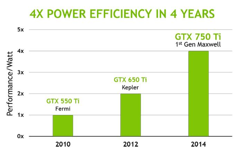
To achieve this NVIDIA has taken a number of steps, some of which they’ve shared with us at a high level and some of which they haven’t. NVIDIA is taking a bit of a “secret sauce” approach to Maxwell from a design level, so while we know a fair bit about its execution model we don’t know quite as much about the little changes that add up to Maxwell’s energy and space savings. However NVIDIA tells us that overall they’ve been able to outright double their performance-per-watt on Maxwell versus Kepler, which is nothing short of amazing given the fact that all of this is being done on the same 28nm process as Kepler.
We’ll go over execution flow and the other gritty details on the next page, but for now let’s start with a look at NVIDIA’s Streaming Multiprocessor designs for Kepler (SMX) and Maxwell (SMM).
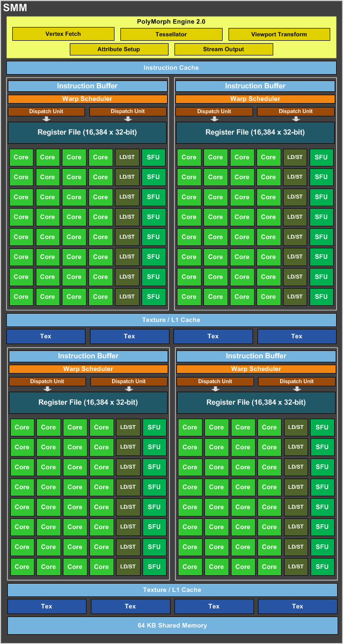
Immediately we can see a significant difference in the layout between the SMX and the new SMM. Whereas the SMX was for all practical purposes a large, flat design with 4 warp schedulers and 15 different execution blocks, the SMM has been heavily partitioned. Physically each SMM is still one contiguous unit, not really all that different from an SMX. But logically the execution blocks which each warp scheduler can access have been greatly curtailed.
The end result is that in an SMX the 4 warp schedulers would share most of their execution resources and work out which warp was on which execution resource for any given cycle. But on an SMM, the warp schedulers are removed from each other and given complete dominion over a far smaller collection of execution resources. No longer do warp schedulers have to share FP32 CUDA cores, special function units, or load/store units, as each of those is replicated across each partition. Only texture units and FP64 CUDA cores are shared.
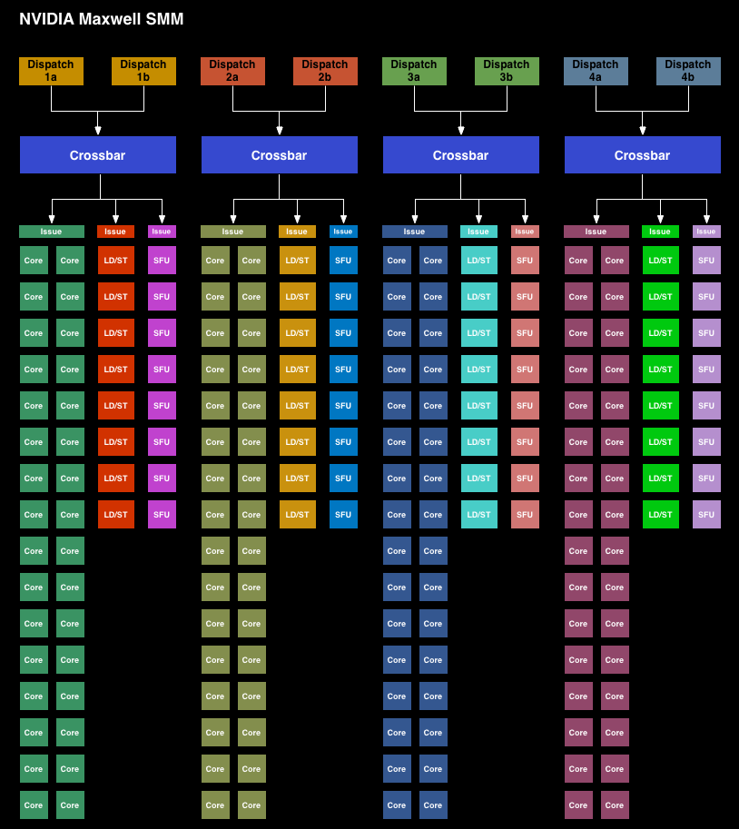
Among the changes NVIDIA made to reduce power consumption, this is among the greatest. Shared resources, though extremely useful when you have the workloads to fill them, do have drawbacks. They’re wasting space and power if not fed, the crossbar to connect all of them is not particularly cheap on a power or area basis, and there is additional scheduling overhead from having to coordinate the actions of those warp schedulers. By forgoing the shared resources NVIDIA loses out on some of the performance benefits from the design, but what they gain in power and space efficiency more than makes up for it.
NVIDIA hasn’t given us hard numbers on SMM power efficiency, but for space efficiency a single 128 CUDA core SMM can deliver 90% of the performance of a 192 CUDA core SMX at a much smaller size.
Moving on, along with the SMM layout changes NVIDIA has also made a number of small tweaks to improve the IPC of the GPU. The scheduler has been rewritten to avoid stalls and otherwise behave more intelligently. Furthermore by achieving higher utilization of their existing hardware, NVIDIA doesn’t need as many functional units to hit their desired performance targets, which in turn saves on space and ultimately power consumption.
While on the subject of performance efficiency, NVIDIA has also been working on memory efficiency too. From a performance perspective GDDR5 is very powerful, however it’s also very power hungry, especially in comparison to DDR3. With GM107 in particular being a 128-bit design that would need to compete with the likes of the 192-bit GK106, NVIDIA has massively increased the amount of L2 cache they use, from 256KB in GK107 to 2MB on GM107. This reduces the amount of traffic that needs to cross the memory bus, reducing both the power spent on the memory bus and the need for a larger memory bus altogether.
Increasing the amount of cache always represents an interesting tradeoff since cache is something of a known quantity and is rather dense, but it’s only useful if there are memory stalls or other memory operations that it can cover. Consequently we often see cache implemented in relation to whether there are any other optimizations available. In some cases it makes more sense to use the transistors to build more functional units, and in other cases it makes sense to build the cache. After staying relatively stagnant on their cache sizes for so long, it looks like the balance has finally shifted and the cache increase makes the most sense for NVIDIA.
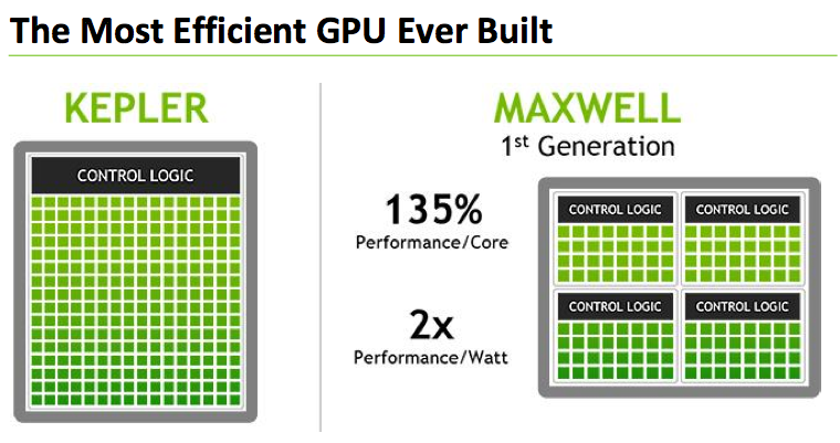
Of course even these changes are relatively high level from an ASIC perspective. There’s always the possibility for low-level changes and NVIDIA has followed through on these too. Case in point, both NVIDIA and AMD have been steadily improving their clock gating capabilities, and with Maxwell NVIDIA has taken another step in their designs. NVIDIA isn’t telling us just how fine grained their gating is now for Maxwell, but it’s a finer granularity than it was on Kepler. Given the new SM design, the most likely change was likely the ability to control the individual partitions and/or the functional units within those partitions, but this is just supposition on our part.
Finally there’s the lowest of low level optimizations, which is transistor level optimizations. Again NVIDIA hasn’t provided a ton of details here, but they tell us they’ve gone through at the transistor level to squeeze out additional energy efficiency as they could find it. Given that TSMC 28nm is now a very mature process with well understood abilities and quirks, NVIDIA should be able to design and build their circuits to a tighter tolerance now than they would have been able to when working on GK107 over 2 years ago.


177 Comments
View All Comments
RealiBrad - Tuesday, February 18, 2014 - link
If you were to run the AMD card 10hrs a day with the avg cost of electricity in the US, you would pay around $22 more a year in electricity. The AMD card gives a %19 boost in power for a %24.5 boost in power usage. That means that the Nvidia card is around %5 more efficient. Its nice that they got the power envelope so low, but if you look at the numbers, not huge.The biggest factor is the supply coming out of AMD. Unless they start making more cards, the the 750Ti will be the better buy.
Homeles - Tuesday, February 18, 2014 - link
Your comment is very out of touch with reality, in regards to power consumption/efficiency:http://www.techpowerup.com/reviews/NVIDIA/GeForce_...
It is huge.
mabellon - Tuesday, February 18, 2014 - link
Thank you for that link. That's an insane improvement. Can't wait to see 20nm high end Maxwell SKUs.happycamperjack - Wednesday, February 19, 2014 - link
That's for gaming only, it's compute performance/watt is still horrible compared to AMD though. I wonder when can Nvidia catch up.bexxx - Wednesday, February 19, 2014 - link
http://media.bestofmicro.com/9/Q/422846/original/L...260kh/s at 60 watts is actually very high, that is basically matching 290x in kh/watt ~1000/280watts, and beating out r7 265 or anything... if you only look at kh/watt.
ninjaquick - Thursday, February 20, 2014 - link
To be honest, all nvidia did was increase the granularity of power gating and core states, so in the event of pure burn, the TDP is hit, and the perf will (theoretically) droop.The reason the real world benefits from this is simply the way rendering works, under DX11. Commands are fast and simple, so increasing the number of parallel queues allows for faster completion and lower power (Average). So the TDP is right, even if the working wattage per frame is just as high as any other GPU. AMD doesn't have that granularity implemented in GCN yet, though they do have the tech for it.
I think this is fairly silly, Nvidia is just riding the coat-tails of massive GPU stalling on frame-present.
elerick - Tuesday, February 18, 2014 - link
Since the performance charts have 650TI Boost i looked up the TDP of 140W. When compared to the Maxwell 750TI with 60W TDP I am in awe of the performance per watt. I sincerely hope that the 760/770/780 with 20nm to give the performance a sharper edge but even if they are not it will still give people with older graphics cards more of a reason to finally upgrade since driver performance tuning will start favoring Maxwell over the next few years.Lonyo - Tuesday, February 18, 2014 - link
The 650TI/TI Boost aren't cards designed to be efficient. They are cut down cards with sections of the GPU disabled. While 2x perf per watt might be somewhat impressive, it's not that impressive given the comparison is made to inefficient cards.Comparing it to something like a GTX650 regular, which is a fully enabled GPU, might be more apt of a comparison, and probably wouldn't give the same perf/watt increases.
elerick - Tuesday, February 18, 2014 - link
Thanks, I haven't been following lower end model cards for either camp. I usually buy $200-$300 class cards.bexxx - Thursday, February 20, 2014 - link
Still just over 1.8x higher perf/watt: http://www.techpowerup.com/reviews/NVIDIA/GeForce_...