The NVIDIA GeForce GTX 750 Ti and GTX 750 Review: Maxwell Makes Its Move
by Ryan Smith & Ganesh T S on February 18, 2014 9:00 AM ESTGeForce GTX 750 Ti & GTX 750 Specifications & Positioning
Having finally covered the architecture and design choices of Maxwell in-depth, let’s talk about the retail hardware itself. As me mentioned in our introduction NVIDIA’s first play with Maxwell will be the high volume markets that GK107 resides in. Ultimately this means we should end up seeing GM107 in mobile GeForce and in server GRID products too, but first NVIDIA is starting with the desktop video card market. The desktop market affords NVIDIA the chance to take more direct control, so while server and mobile products go through additional phases of OEM/partner validation, desktop can be the first up to bat.
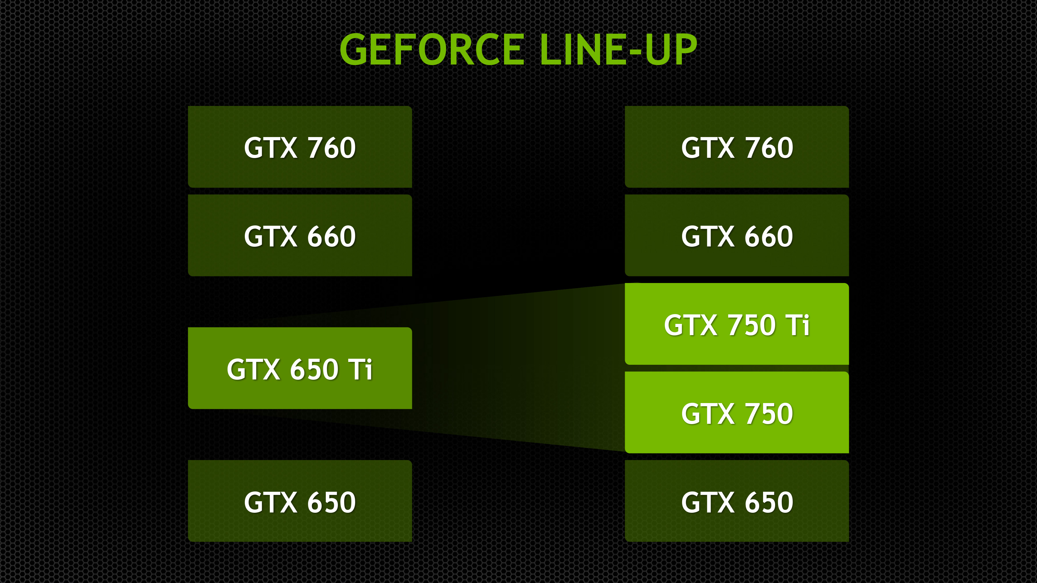
In a move a bit different from usual for an NVIDIA desktop video card launch, NVIDIA is launching multiple GM107 cards at once. Typically they’d stretch this out over a couple of weeks, but with the 700 series already on the market (and nothing better to do with salvaged chips) there’s little reason to wait.
| NVIDIA GPU Specification Comparison | ||||||
| GTX 660 | GTX 750 Ti | GTX 750 | GTX 650 | |||
| CUDA Cores | 960 | 640 | 512 | 384 | ||
| Texture Units | 80 | 40 | 32 | 32 | ||
| ROPs | 24 | 16 | 16 | 16 | ||
| Core Clock | 980MHz | 1020MHz | 1020MHz | 1058MHz | ||
| Boost Clock | 1033MHz | 1085MHz | 1085MHz | N/A | ||
| Memory Clock | 6GHz GDDR5 | 5.4GHz GDDR5 | 5GHz GDDR5 | 5GHz GDDR5 | ||
| Memory Bus Width | 192-bit | 128-bit | 128-bit | 128-bit | ||
| VRAM | 2GB | 2GB | 1GB | 1GB | ||
| FP64 | 1/24 | 1/32 | 1/32 | 1/24 | ||
| TDP | 140W | 60W | 55W | 64W | ||
| Transistor Count | 2.54B | 1.87B | 1.87B | 1.3B | ||
| Manufacturing Process | TSMC 28nm | TSMC 28nm | TSMC 28nm | TSMC 28nm | ||
| Architecture | Kepler | Maxwell | Maxwell | Kepler | ||
| GPU | GK106 | GM107 | GM107 | GK107 | ||
| Launch Date | 09/13/12 | 02/18/14 | 02/18/14 | 09/13/12 | ||
| Launch Price | $229 | $149 | $119 | $109 | ||
Starting with the GeForce GTX 750 Ti, this is NVIDIA’s flagship GM107 product. GTX 750 Ti packs a complete GM107 implementation, comprising 5 SMMs, 640 CUDA cores, 16 ROPs, and 40 texture units, and fed by 2MB of L2 cache. In terms of design GM107 is a clear successor to GK107, as evidenced by use of just 16 ROPs.
Nevertheless it’s very important to keep in mind that thanks to the Maxwell architecture GM107 hits well above its weight, so the CUDA core count difference between the GTX 750 Ti and GTX 660 makes these parts look much farther apart than they actually are. At least so long as we’re comparing Kepler and Maxwell parts, the product number is going to be the more meaningful designation as specs alone will not capture the relative power and efficiency of these designs.
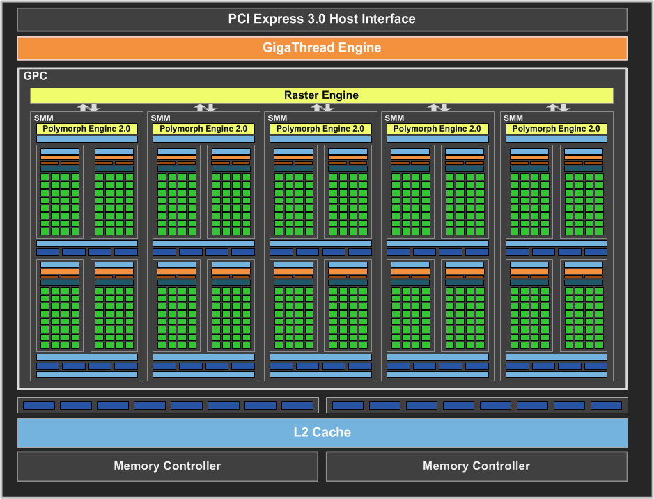
GTX 750 Ti Block Diagram
GTX 750 Ti’s GM107 GPU is in turn paired with 2GB of GDDR5, on a 128-bit bus. The use of 2GB of VRAM is common for cards at this price range, whereas the 128-bit bus is narrower than competing cards, but something NVIDIA doesn’t expect to be badly hindered by due to their efficiency improvements elsewhere. On the other hand the company also expects some of its partners to roll out a smaller numbers of 1GB cards in the near future, and while these will be $10 cheaper we’re of the opinion that there’s no reason to have less than 2GB of VRAM on a card in this price range.
When it comes to clockspeeds NVIDIA will be shipping GTX 750 Ti and its GM107 GPU at slightly higher clockspeeds than its Kepler counterparts. NVIDIA is putting the core clock at 1020MHz with an official boost clock of 1085MHz; and as this is a GPU Boost 2.0 we’ll see the highest boost bins top out well over 1100MHz. The VRAM on the other hand will be clocked at 5.4GHz, which on a 128-bit bus is enough to provide 86.4GB/sec of memory bandwidth. The use of 5.4GHz RAM here is a bit off an oddity since no one produces GDDR5 RAM at that speed bin – these cards will have to be equipped with 6GHz RAM in order to meet the required specifications – so we strongly suspect this is a board limitation, especially since the board is virtually identical to NVIDIA’s board design for GTX 650 Ti, which also has the same 5.4GHz memory clock.
Switching gears for a moment, let’s now cover the GTX 750. GTX 750 is based on a cut-down/salvaged GM107 GPU, utilizing just 4 of GM107’s 5 SMMs. This reduces the CUDA core count to 512 and the number of texture units to 32, but it leaves the ROP/L2/memory partitions fully intact. GPU clockspeeds are identical to GTX 750 Ti – 1020MHz base, 1085MHz boost – while the memory subsystem is further reduced to 1GB of GDDR5 running at 5GHz. As such, the GTX 750 will fall behind the 750 Ti by anywhere between 8% and 20%, depending on whether the workload being measured is memory bound or shader/texture bound.
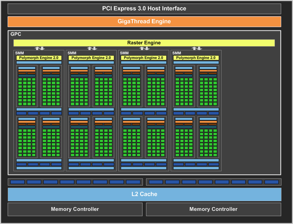
GTX 750 Block Diagram
But perhaps the most impressive metric is power consumption. Due to NVIDIA’s optimizations efforts and 2x perf-per-watt goal for Maxwell, power consumption is way down versus the GK106 based parts that the GTX 750 and GTX 750 Ti will be replacing. NVIDIA’s official TDP – which is generally comparable within the NVIDIA product lineup – is just 60W for GTX 750 Ti, and a lower still 55W for GTX 750. For the sake of comparison this is a bit lower than either GTX 650 or GT 640 (the desktop GK107 parts), and more importantly these new GTX 750 series cards are quite a bit more powerful than the GK107 cards at similar TDPs.
The end result is that we’re looking at either a significant reduction in power consumption for similar performance to GK106, or a massive increase in performance as compared to GK107. Given the power limited nature of mobile in particular, this makes GM107 an especially potent GPU for NVIDIA.
With that in mind, it’s interesting to note that all of this comes despite the fact that both transistor counts and die sizes are up compared to GK107. GK107 was 118mm2 for 1.3 billion transistors, and meanwhile GM107 is 148mm2 for 1.87B transistors. The fact that NVIDIA was able to increase their transistor count by 43% has a lot to with how much faster GM107 is than GK107, but at the same time the fact that die size itself is only up by 25% showcases those die size optimizations we talked about earlier.
Ultimately when we’re on a single node – this is all TSMC 28nm HP, not HPM – there’s typically a loose correlation between die size and power consumption in a chip stack, which is something NVIDIA has been able to dodge with GM107. Due to all of their power optimizations NVIDIA has been able to grow GK107 to GM107 essentially for free, and this still doesn’t take into account the higher IPC of Maxwell.
NVIDIA's Product Positioning
With up to 640 CUDA cores that hit above their weight and a TDP below 75W, GTX 750 Ti and GTX 750 will be filling a duo of roles in the NVIDIA lineup. From a performance and price standpoint NVIDIA is placing them between the GK106 flagship GTX 660 and the GK107 flagship GTX 650. GTX 750 Ti isn’t quite fast enough to displace GTX 660, so GTX 660 continues to live for another day while NVIDIA uses GTX 750 Ti to retire GTX 650 Ti Boost, and GTX 750 to retire GTX 650 Ti. Both of those were based on cut-down GK106 GPUs, so there’s an immediate benefit to NVIDIA of reducing production costs, and for consumers these new GTX 750 series cards will be faster than the cards they replace by roughly the same performance factor as we’ve seen elsewhere for GTX 700 series cards. Elsewhere GTX 650 and below will also live for another day as budget offerings, due to GK107’s smaller die size and lower production costs.
Meanwhile these sub-75W TDPs means that the GTX 750 series are now going to be NVIDIA’s best cards for the sub-75W PCIe bus powered only market. GTX 650, despite its TDP, required a 6pin PCIe power connector, so in that space the GTX 750 series is replacing the even slower GT 640 (GK107 + DDR3) as NVIDIA’s top card. For the purposes of the desktop video card space this puts the GTX 750 series squarely in the middle of the HTPC space and OEM upgrade space.
The HTPC space has long favored sub-75W cards for noise and space reasons, and NVIDIA’s video decode power improvements should be further welcome in this space. In this sense NVIDIA’s petite products for smaller form factor computers will be an interesting split between the reference GTX 780 and the GTX 750 series. Reference GTX 780 being well suited for small form factor designs due to its well-constructed blower, and the GTX 750 series being well suited for very low power designs or designs that don’t meet the air intake requirements for a blower.
As for the OEM upgrade space, this is a fairly straightforward but large market. The two sweet spots for video card upgrades for OEM systems are sub-150W cards for the OEMs that supply a single PCIe power plug (some of them), and sub-75W cards for OEMs that don’t supply a PCIe power plug, or even a very powerful PSU in the first place (more of them). These scenarios are fundamentally power limited – not unlike mobile – so having the fastest card at sub-150W and sub-75W is potentially very good for business. In NVIDIA’s case they are making a clear play for the sub-75W market with these cards, and one of their marketing pushes will be to go after OEM upgrades.
That said, whenever we’re talking about mainstream cards the Asia-Pacific (APAC) market becomes especially important due to its size and higher price sensitivity. Countries like China have been strong markets for cards like the GTX 750 series, so NVIDIA is expecting much of the same here. Once again NVIDIA’s strongest play will be the sub-75W market given their power advantage, as in unrestricted power scenarios AMD will have the upper hand. The wild card factor here will be APAC’s far greater use of internet cafes and LAN gaming centers, as operators are likely to be more interested in power consumption when it’s spread out over numerous computers.
Pricing & Competitive Landscape
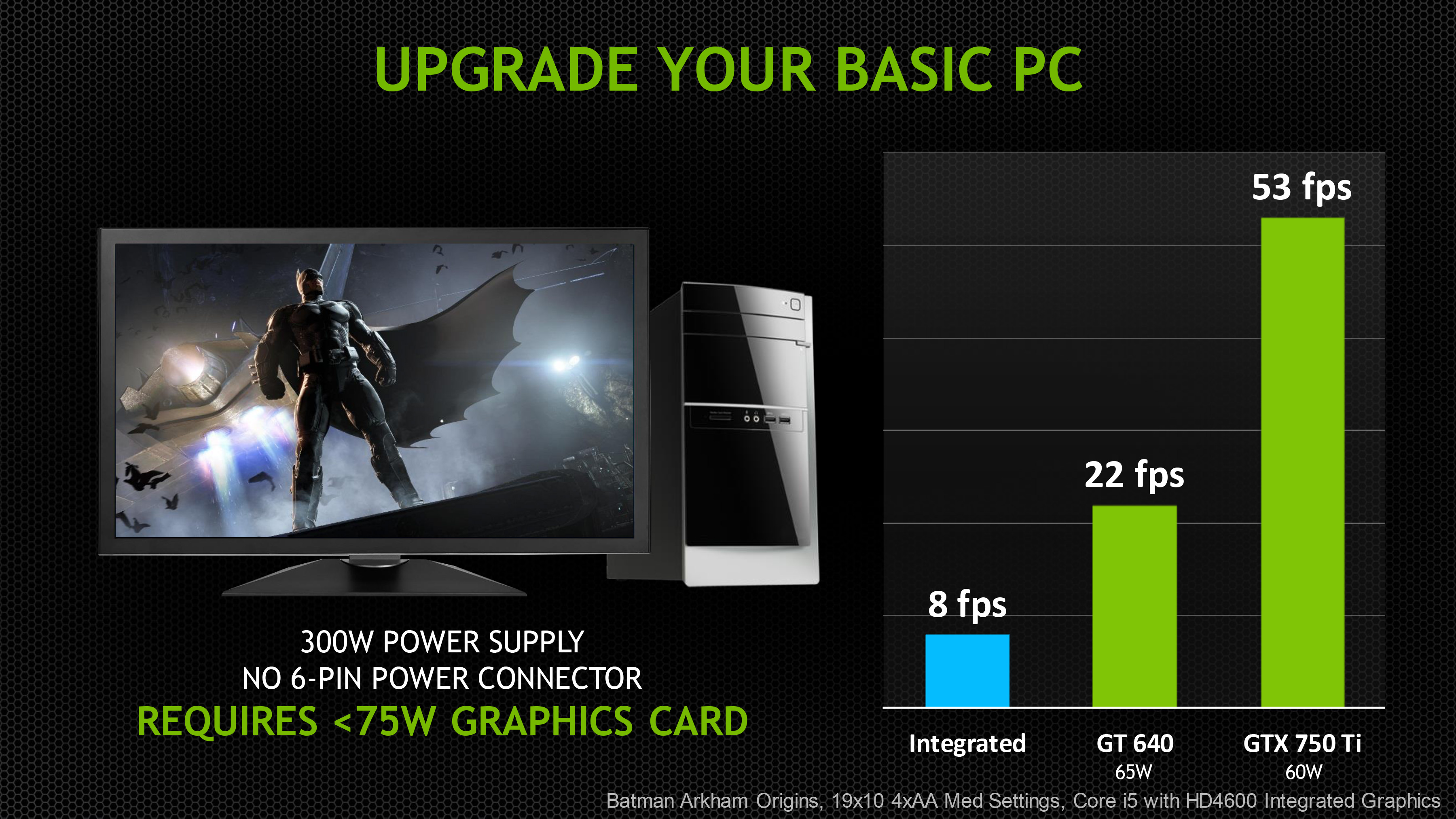
Wrapping things up, the GTX 750 series will be a hard launch with immediate availability on a global scale. NVIDIA is placing the MSRP for the GTX 750 Ti at $149 and the MSRP for the GTX 750 at $119, right between the GTX 660 and GTX 650, while pushing GTX 650 Ti out of the picture entirely. From a performance perspective these cards won’t offer the kind of performance that will entice most 600 series owners to upgrade (though the performance gains against GT 640 are striking), but NVIDIA is making a major effort to target GTX 550 Ti and GTS 450 owners as those cards turn 3-4 years old, with the GTX 750 series able to easily double their performance while reducing power consumption.
AMD’s competition for the GTX 750 series will be the recently launched Radeon R7 265, and the recently price dropped Radeon R7 260X, which are set to go for $149 and $119 respectively. Unfortunately R7 265 was not a hard launch and is not expected until the end of this month, so NVIDIA is going to have roughly two weeks of availability ahead of AMD at $149, and meanwhile at $119 we’re still waiting to see the announced price cuts take effect.
From a price/performance standpoint NVIDIA is not going to be especially competitive, and this is similar to how NVIDIA handled the mainstream cards in the 600 series. NVIDIA is content to take second place on a price/performance basis, relying on their stronger brand name and greater brick & mortar retail presence to make up for what they lose from lower performance, a strategy that apparently worked well for the 600 series. Accordingly, once they hit the market (and assuming they stay at MSRP), R7 265 and R7 260X will be faster than their GTX 750 series’ counterparts, as AMD is just outright throwing more hardware at the problem. But as a result AMD will not be able to compete with NVIDIA’s power efficiency; in those sub-75W markets NVIDIA will have the more powerful (and more expensive) options.
| Winter 2014 GPU Pricing Comparison | |||||
| AMD | Price | NVIDIA | |||
| Radeon R9 270 | $250 | GeForce GTX 760 | |||
| $190 | GeForce GTX 660 | ||||
| Radeon R7 265 | $150 | GeForce GTX 750 Ti | |||
| Radeon R7 260 | $130 | ||||
| Radeon R7 260X (New MSRP) | $120 | GeForce GTX 750 | |||
| Radeon R7 250X | $100 | GeForce GTX 650 | |||
| Radeon R7 250 | $90 | GeForce GT 640 | |||


177 Comments
View All Comments
Harag - Thursday, March 6, 2014 - link
Not true at all. The release of the Titan showed they could unlock FP64 performance on a specific architecture. The Titan Black also has amazing FP64 performance. You may also want to look into their Quadro line.kwrzesien - Tuesday, February 18, 2014 - link
Cards are available on Newegg! Check out this EVGA Superclocked (1268MHz) with a dual-fan ACX cooler and 6-pin PCIe power connector: http://www.newegg.com/Product/Product.aspx?Item=N8...Frenetic Pony - Tuesday, February 18, 2014 - link
Maxwell is designed for mobile gaming, in which case who cares? Broadwell looks to improve performance per watt at least as much as Maxwell if Intel's initial hints of 30% power improvement for 14nm and 40% improvement for gpu power efficiency pan out. And they were already damned good.But Maxwell isn't designed for high end, in which case GCN 1.1 and AMD are already beating them for price for performance. Congrats Nvidia, you're second place in both categories if this card is anything to go by. I hope to hell your Titan 2 or whatever kicks more ass than this card.
varad - Wednesday, February 19, 2014 - link
@FreneticPony, statements like "Maxwell is designed for mobile gaming" and "But Maxwell isn't designed for high end" tell us you know precious little. Maxwell is an architecture that will span across all of Nvidia's products [Tegra, GeForce, Quadro and Tesla].Frenetic Pony - Thursday, February 20, 2014 - link
Err... they intend to produce as such yes. But it's obvious the architecture itself is targeted squarely at mobile. Power constraints don't actually get in the way as much as other constraints do on the high end. Who really cares if it's 150+ tdp if it's gaming? You get constrained by memory latency and other things no matter how high you can clock it up.This appears to be Nvidia's version of Haswell, concentrated solely on improving performance per watt rather than performance at all. Which is bad timing as Intel is doing the same, but integrates it's GPUs right onto the chip, making them cheaper and smaller than any dedicated card for a laptop is going to be. Meanwhile AMD is crushing Nvidia in both compute and high end gaming performance on the desktop for performance per $.
True, this will help mitigate electricity cost. for compute based work. But as others pointed out not by much. Meaning Nvidia stuck itself with the wrong focus at the wrong time. Maybe it will help with their Tegra SOCs, if they're lucky they'll get back into the game, as Qualcomm soundly crushed the Tegra 4 for third party ARM Socs over the last year.
So, no, it's designed for high end. Doesn't mean they're not going to do it anyway.
Frenetic Pony - Thursday, February 20, 2014 - link
I.E. it really doesn't matter how well they did at what they're doing. Because Intel has done just as well and has built in advantages for its market, what their doing doesn't help that much against AMD in the high end market, and this leaves their only chance for financial success with it being next years Tegra SOCs.ninjaquick - Thursday, February 20, 2014 - link
Plus, AMD is easily capable of taking Nvidia on at the low end with better hardware across the board, more integrated designs, etc.willis936 - Thursday, February 20, 2014 - link
Pro tip: you're always TDP limited. Increasing performance per watt IS increasing performance.Harag - Thursday, March 6, 2014 - link
Broad statements like "AMD is crushing Nvidia..." only proved @Varad correct. you know precious little.HisDivineOrder - Wednesday, February 19, 2014 - link
nVidia fits a lot more performance in a little more space at a lot less power and you think they're doing poorly? This is on the same node.Imagine what they'll pack into a smaller node.
Their focus is probably the right one, given the fact they want to migrate these cores into Tegra.