Intel Readying 15-core Xeon E7 v2
by Ian Cutress on February 11, 2014 1:32 PM EST
Reports from ISSCC are coming out that Intel is preparing to launch a 15-core Xeon CPU. The 15-core model was postulated before Ivy Bridge-E launch, along with 12-core and 10-core models – the latter two are currently on the market but Intel was rather silent on the 15-core SKU, presumably because it harder to manufacturer one with the right voltage characteristics. Releasing a 15-core SKU is a little odd, and one would assume is most likely a 16-core model with one of the cores disabled – based on Intel’s history I doubt this core will be able to be re-enabled should the silicon still work. I just received the official documents and the 15 core SKU is natively 15-core.
Information from the original source on the top end CPU is as follows:
- 4.31 billion transistors
- Will be in the Xeon E7 line-up, suited for 4P/8P systems (8 * 15 * 2 = 240 threads potential)
- 2.8 GHz Turbo Frequency (though the design will scale to 3.8 GHz)
- 150W TDP
- 40 PCIe lanes
Judging by the available information, it would seem that Intel are preparing a stack of ‘Ivytown’ processors along this design, and thus a range of Xeon E7 processors, from 1.4 GHz to 3.8 GHz, drawing between 40W and 150W, similar to the Xeon E5 v2 range.
Predictions have Ivytown to be announced next week, with these details being part of the ISSCC conference talks. In comparison to some of the other Xeon CPUs available, as well as the last generation:
| Intel Xeon Comparison | |||||
| Xeon E3-1280 v3 | Xeon E5-2687W | Xeon E5-2697 v2 | Xeon E7-8870 | Xeon E7-8890 v2 | |
| Socket | LGA1150 | LGA2011 | LGA2011 | LGA1567 | LGA2011 |
| Architecture | Haswell | Sandy Bridge-EP | Ivy Bridge-EP | Westmere-EX | Ivy Bridge-EX |
| Codename | Denlow | Romley | Romley | Boxboro | Brickland |
| Cores / Threads | 4 / 8 | 8 / 16 | 12 / 24 | 10 / 20 | 15 / 30 |
| CPU Speed | 3.6 GHz | 3.1 GHz | 2.7 GHz | 2.4 GHz | 2.8 GHz |
| CPU Turbo | 4.0 GHz | 3.8 GHz | 3.5 GHz | 2.8 GHz | 2.8 GHz |
| L3 Cache | 8 MB | 20 MB | 30 MB | 30 MB | 37.5 MB |
| TDP | 82 W | 150 W | 130 W | 130 W | 155 W |
| Memory | DDR3-1600 | DDR3-1600 | DDR3-1866 | DDR3-1600 | DDR3-1600 |
| DIMMs per Channel | 2 | 2 | 2 | 2 | 3 ? |
| Price at Intro | $612 | $1885 | $2614 | $4616 | >$5000 ? |
According to CPU-World, there are 8 members of the Xeon E7-8xxx v2 range planned, from 6 to 15 cores and 105W to 155W, along with some E7-4xxx v2 also featuring 15 core models, with 2.8 GHz being the top 15-core model speed at 155W.
All this is tentative until Intel makes a formal announcement, but there is clearly room at the high end. The tradeoff is always between core density and frequency, with the higher frequency models having lower core counts in order to offset power usage. If we get more information from ISSCC we will let you know.
Original Source: PCWorld
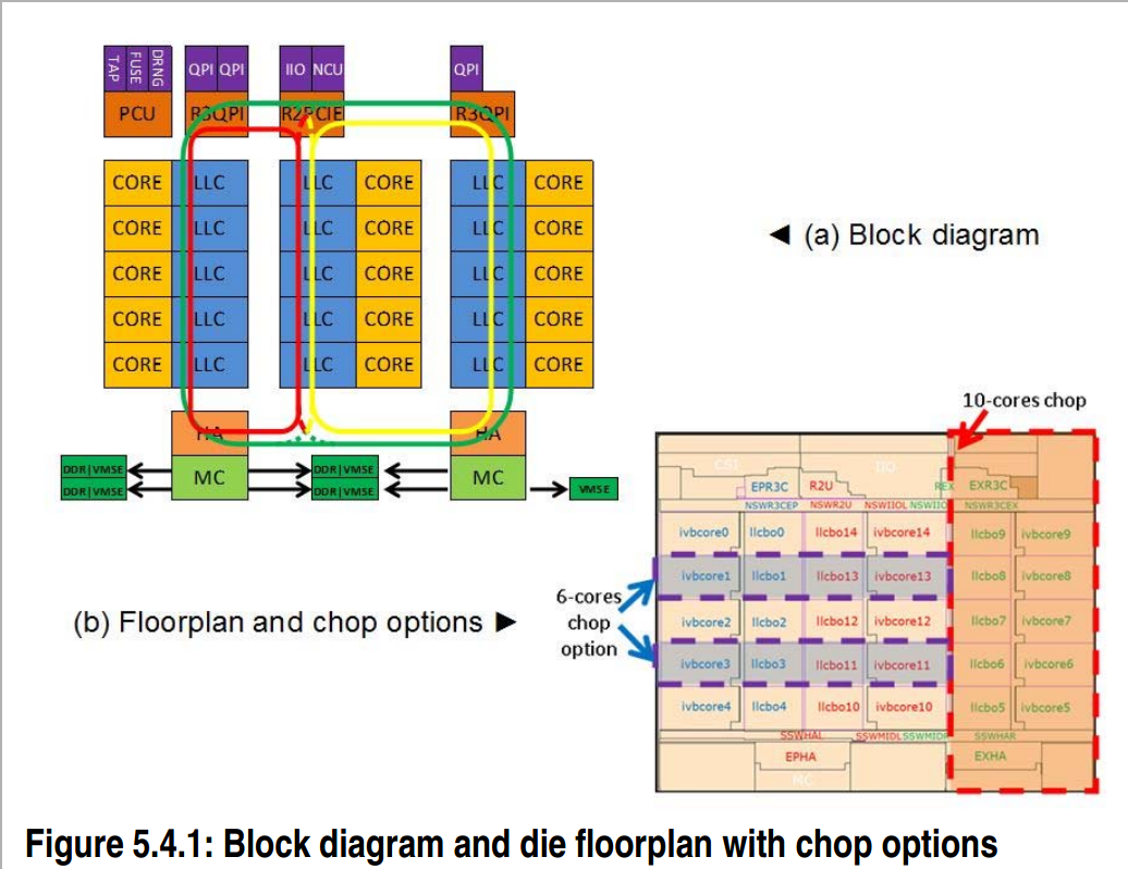
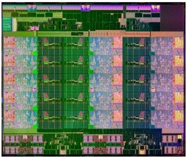
Update: Now I have time to study the document supplied by Intel for ISSCC, we can confirm the 15-core model with 37.5 MB L3 cache, using 22nm Hi-K metal-gate tri-gate 22nm CMOS with 9 metal layers. All the Ivytown processors will be harvested from a single die:
Ivytown Die Shot
The design itself is capable of 40W to 150W, with 1.4 GHz to 3.8 GHz speeds capable. The L3 cache has 15x 2.5MB slices, and data arrays use 0.108µm2 cells with in-line double-error-correction and triple-error-detection (DECTED) with variable latency. The CPU uses three clock domains as well as five voltage domains:
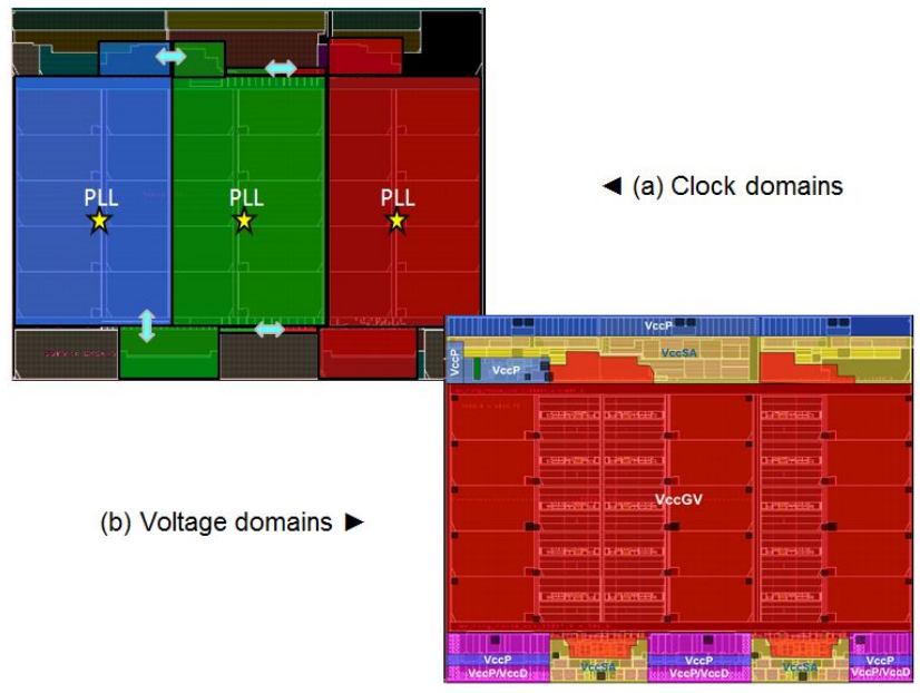
Level shifters are placed between the voltage domains, and the design uses lower-leakage transistors in non-timing-critical paths, acheving 63% use in the cors and 90% in non-core area. Overall, leakage is ~22% of the total power.
The CPUs are indeed LGA2011 (the shift from Westmere-EX, skipping over Sandy Bridge, should make it seem more plausible), and come in a 52.5x51.0mm package with four DDR3 channels. That would make the package 2677 mm2, similar to known Ivy Bridge-E Xeon CPUs.
CPU-World's list of Xeon E7 v2 processors come from, inter alia, this non-Intel document, listing the 105W+ models.


55 Comments
View All Comments
IUU - Sunday, February 16, 2014 - link
Everyone is sick of the 6 and 8 cores, or the 4 cores as mainstream. They seem to be in the market for an eternity. You can't exactly blame fully Intel for this as really multithreaded programs are still a scarcity.You can't exactly blame programmers as well because their compensation is ridiculous and their job inhumanly demanding.About this "power user" thing; it is dumb to self hallucinate that there is the average joe as opposed to "high performance" computing, the"big data" or "science apps". Remember that people in these fields readily salivate for gamer's gpus and be frank to recognize that supercomputing would have much less progress if it weren't for the poor average joe that you seem to scorn.
The fact that 12-15 cores are available for " businesses" but not for the average joe is a travesty that stinks of decadence, waiting for the next paradigm of innovation.
twtech - Thursday, February 20, 2014 - link
This is a bit of a chicken and egg problem, both for the hardware, and for the fact that the threading support in C++ is still relatively poor - it doesn't really have much in the way of features designed to help deal with the data-access control problem that is big issue in multithreaded programs (and C++ is still the language of choice for performance-critical apps, the likes of which would have a potential benefit from better usage of threading in the first place).sanaris - Monday, February 17, 2014 - link
Virtualization and cloud - nah.Production - yes.
I need as much as possible power inside single motherboard to run quantum predictions.
Jaybus - Wednesday, April 8, 2015 - link
Then go for more PCIe lanes for GPUs and OpenCL, rather than more SMP cores.psyq321 - Wednesday, February 12, 2014 - link
It is not the same LGA 2011 socket as Xeon E5 / Core i7 49xx unfortunately.This is due to different memory controller, so the pin layout is different and, thus, not compatible.
Kevin G - Tuesday, February 11, 2014 - link
I'm rather surprised if they go with the same socket 2011 as SandyBridge-E/Ivy Bridge-E. One of the hallmarks of the EX line has been its good socket scalablity by having 4 QPI links. This enables 8 socket systems with minimal hops between sockets. Similarly the EX has used memory buffers to enable more bandwidth and higher memory capacities than the EP line.If the included picture hasn't been modified by Photoshop, then we're looking at a different physical key for the socket.
Ian Cutress - Tuesday, February 11, 2014 - link
To quote Intel's paper at ISSCC: "The processor supports two 2011-land, 40-mil pitch organic flip-chip LGA package options", which I would interpret as LGA-2011.Kevin G - Tuesday, February 11, 2014 - link
Yes, it has 2011 pads on the package. Rather are they configured the same as SandyBridge-E/Ivy Bridge-E. In other words, does it have two QPI links, four DDR3 channels and 40 PCI-e lanes as the main IO features?Also worth pointing out is that the rumors of Haswell-E have it using a 2011 pad package as well but supporting DDR4 memory. This variant has been tagged as 2011v3. (Presumably Ivy Bridge-EX would be 2011v2.)
Kevin G - Tuesday, February 11, 2014 - link
Actually looking at the block diagram, something is really weird. What is VSME and why are there seven of the links? Could these be a new serial memory bus technology? I'd fathom it'd be useful for a spare memory channel in a RAID5-like array (See the Alpha EV7). However, everything else points to two independent memory controllers which complicate such a function.Further more, the block diagram indicates 3 QPI links which would allow this chip to scale to 8 sockets. The current Sandy Bridge-E/Ivy Bridge-E only go upto quad socket.
I wonder if Intel has some something rather crazy: enabled this die to be used in both the original LGA 2011 and a new EX variant. All the 12 core Ivy Bridge-E's were rumored to be using this die.
psyq321 - Wednesday, February 12, 2014 - link
It is probably the same die shared between HCC EP and EX lines, but with different modules being enabled in EX line (extra QPI, etc.)It could also be that Intel originally planned 15 core Ivy Bridge EP but decided to keep 15 core SKU only for the EX generation.
In any case, we are now stuck with 3 different LGA2011 configurations:
- LGA2011 - for Sandy Bridge EP / Ivy Bridge EP
- LGA2011-1 - for Ivy Bridge EX and Haswell EX
- LGA2011-3 - for Haswell EP (and maybe Broadwell EP)
Last two can support DDR4, but the memory configuration in EX line is totally different, and goes through a scalable memory buffer.
Way to keep things simple :)