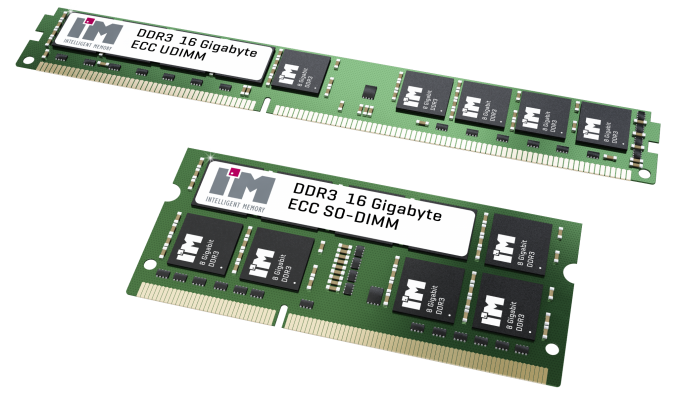
I'M Intelligent Memory to release 16GB Unregistered DDR3 Modules
by Ian Cutress on February 11, 2014 6:59 PM EST- Posted in
- Memory
- Modules
- 16GB
- 8Gb
- I'M Intelligent Memory
After talking about Avoton and Bay Trail on Twitter, I was approached by the company heading up the marketing and PR for I’M Intelligent Memory regarding a few new products in the pipeline different to what we had seen in the market previously. The big one in my book is that they are currently sampling 16GB unregistered DDR3 modules ready for ramping up production.
Currently in the consumer space we have 8GB unregistered modules, usually paired together for a 16GB kit. These use sixteen 4 Gb memory packages on board to total up to the 8 GB number, and are packaged in speeds up to 2933+ MT/s. Intelligent Memory are a company (or series of smaller individual companies) that have new IP in the market to tie two of these 4 Gb dies together into a 8 Gb die, and are thus able to double the capacity of memory available in the market.
I have been speaking with Thorsten Wronski, President of Sales and Technology at Memphis AG, the company heading up the business end of the Intelligent Memory plan. We went into detail regarding how the new IP works (as much as I could be told without breaking NDA):
DRAM stacking is unlike NAND stacking. We have seen manufacturers stick 16 NAND dies onto a single package, but DRAM requires precise (picosecond level) timing to allow the two 4 Gb dies to act as a single 8 Gb package. This is the new IP to the table, which can apply to both unregistered and registered memory, as well as ECC memory.
The JEDEC specifications for DDR3 do account for the use of 8 Gbit packages (either one 8 Gbit die or two 4 Gbit dies per package), should these be available. However I am told that currently there is a fundamental non-fixable issue on all Intel processors (except Avoton and Rangeley, other Silvermont (BayTrail) is affected) that means that these dies are not recognised. In their specifications for Ivy Bridge-E, Intel do state that 8Gb packages are supported (link, page 10), however this apparently has not been the case so far and I'M is working with motherboard manufacturers to further pin down this issue.
Typically the access of a memory chip requires a column and a row, both of which are multiplexed across a set of 16 connects. With a 4 Gbit package, to access the row, all 16 are used (A0 to A15), whereas a column uses 10 (A0 to A9). In the 8 Gbit package, the column also requires A11, all part of the JEDEC spec. This works on Avoton/Rangeley, but not on any other Intel processor, according to Intelligent Memory, and the exact nature of the issue is down to Intel’s implementation of the specification. I suspect that Intel did not predict 8 Gbit packages coming to market at this time, and have found an efficiency improvement somewhere along the line. Perhaps needless to say, Intel should be supporting the larger dies going forward.
The dies that I’M are using are 30nm, and according to them the reason why Hynix/Samsung et al have not released an 8 Gbit DRAM die up until this point is that they are waiting until 25nm in order to do so – this is why I’M is very excited about their product. It could also mean that users wanting HSA implementations under Kaveri could have access to 64GB of DRAM to play with. But it also means that when 8 Gbit 25nm DRAM dies become available, I’M will perhaps try for a 16 Gbit package for 32GB modules - all aimed for DDR4 I would imagine.
I’M Intelligent Memory is currently a couple of weeks out from sampling our server guru Johan with some of these modules, so hopefully we will get an insight from him as to how they are looking. They are intending to go down two routes with their product – selling the combined die packages and selling modules. I have been told that one of the normal end-user manufacturers has already expressed interest in the packages (rated at DDR3-1600), which they would place onto their own DRAM sticks and perhaps bin the ICs for higher speed. The modules will be sold also via a third-party that often deals in bulk sales.
Mass production is set to begin in March and April, with initial pricing per 16GB module in the $320-$350 range for both DIMM and SO-DIMM, ECC being on the higher end of that range. To put that into perspective, most DRAM modules on sale today for end-users are in the $8-$14/GB range, making the modules have a small premium which is understandable to get the higher density.
If this IP holds up to the standard, I would not be surprised if it is purchased (or at the very least observed) by the big DRAM manufacturers. I expect these modules will first see the light of day in servers (Avoton based most likely), and I will keep an eye out if any end-user manufacturers get a hold of some. I’M have verified the modules on AMD FX processors (FX-6300 and FX-8320 on 990FX/AM3+) as well as AMD's 760G and A75 (FM2 socket) chipsets. I was forwarded the following screenshot of two of these modules in an MSI FM2-A75MA-P33 motherboard, which is a dual DRAM module motherboard using the FM2 socket for Trinity APUs:
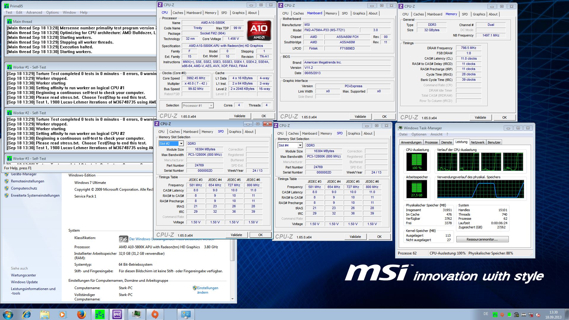
Here each of the 16GB modules (shown in the SPD tab of CPU-Z) are running at DDR3-1600 11-11-11, giving the two DRAM slot motherboard a total of 32GB of addressable space.
Aside from unregistered modules, I’M are also planning ECC UDIMM and RDIMM versions as well, such as 16GB very-low-profile RDIMMs and 16GB ECC SO-DIMMs. Non ECC SO-DIMMs are also being planned. A lot of their focus will be the supply of DRAM components for the direct integration onto automated systems where memory counts are fixed, for systems that use Marvell, TI, Freescale, Xilinx, Altera, Renesas and so on.


61 Comments
View All Comments
Lone Ranger - Wednesday, February 12, 2014 - link
A few people here are implying that Intel screwed up by not implementing support for the larger DIMMs, even though it is in the JEDEC spec. It very well may be intentional, as to not cannibalize their low end Xeon sales (E3 series).KAlmquist - Wednesday, February 12, 2014 - link
The article indicates that the problem occurs on all Intel processors using DDR-3 except for the Atom models (which presumably use a different memory controller).The maximum memory sizes specified for various Intel processors seem to assume DDR-3 DIMMs no larger than 8GB. LGA1155 and LGA1150 models (including the E3 series) are specified as supporting a maximum memory of 32GB (2 channels times 2 DIMMs/per channel times 8GB per DIMM). Similarly, LGA2111 chips are specified as supporting a maximum memory of 64GB (4 channels instead of 2). So it would seem that the lack of support for 16GB DIMMs is at least partially intentional.
TiGr1982 - Thursday, February 13, 2014 - link
That's a good point; as an argument in favor of that, Intel intentionally cuts ECC memory support for Core i7 to prevent using i7's instead of Xeons.bobbozzo - Wednesday, February 12, 2014 - link
Anyone know if these will work in the HP MicroServer Gen8?Someone tried some 16GB UDIMMs designed for an Apple workstation and they didn't get past POST.
TommyVolt - Thursday, February 13, 2014 - link
HP Microserver Gen8 uses Intel CPU....won't work. But I recommend to write an email to HP telling them about these modules and asking if they would support in the future.I think HP has the power to make Intel move!
Lone Ranger - Friday, February 14, 2014 - link
There is a key combo during POST that bypasses memory checks on some HP servers. Need to search around....mattlach - Thursday, June 26, 2014 - link
I am eagerly looking forward to buying 4 16GB ECC UDIMM's for my basement VMWare ESXi server, but I can't find these anywhere, and the distributors aren't responding to my emails (presumably because I am a small volume individual buyer)Has anyone found these for sale ANYWHERE?
kjboughton - Thursday, July 31, 2014 - link
ASUS have just released a beta BIOS for the X79 DELUXE that is intended to address the general incompatability with Intel SBE/IVE.http://dlcdnet.asus.com/pub/ASUS/mb/LGA2011/X79-De...
q.epsilon.p - Saturday, April 18, 2015 - link
Obviously these are going to be stupid expensive and unless you need 64GB on a 4 slot dual channel bored or 128 on a 8 shot quad channel bored it's completely not going to be worth it.But I'm not doing a total system upgrade to early 2017 when the Cannonlake successor will be launched, as well and AMD Zen will have been out for a bit. Although if the leaks are accurate it looks like AMD is taking the same dumb path they took with Piledriver and packing a s*** ton of cores on a single die rather than making more powerful cores.
Which now we are talking about 16 cores on there APU's and probably 32 cores on there pure x86 processors... which is dumb and I hope the leaks are false as it makes NO sense to have so many cores with hyper threading, meaning with the pure x86 processor it would have 64 threads which is dumb as f***.
We are still having problems with supporting 8 threads in a most applications and if the leak is accurate they want to jump to 64 threads... this is even more stupid than piledriver if the leak is accurate they should be working on IPC not increasing the number of cores sticking with 8 cores and doubling or increasing the intructions per cycle by a little more would be what they need to do.
Bleakwise - Friday, September 11, 2015 - link
Completely disagree. For one, they are working on IPC. Second, 64 threads makes complete sense for many many workloas, especially on the SERVER, and the last time AMD was profitable was when they were competing with Intel in the server space. Guess what the #1 generator of revenue is for Intel? I can assure you it's not gamers buying their k model i5.While IPC will be boosted, even 32 or 64 piledriver threads would be AMAZING for things like Cinibench, content creation, compilation, level design, 3d modeling, sound production, etc etc. Look at say Cubase or Pro Tools, they need CORES not IPC. Or large Visual Studio projects, hundreds of threads get used in build clusters. Look at CryEngine or UE4 or Unity, hundreds of cores go to work on baking lighting.
That said, even in gaming there are many workloads that are thread-bound. Physics for example is being held back by a lack of CPU cores as a complete Physics pipeline on GPU is simply not possible, just eye-candy, because rigid body and game state are too coupled.
AMD is going to be putting large HSA enabled APUs on their Zen cores also, R9 graphics with an HBM cache acting something like the Xbox One's ESRAM. People will be able to buy an AMD APU and game on it, done and with DirectX 12 that is a bigger deal than it was, and being more powerful than consoles they'll be able to play every console port from this generation-- all on a budget.
That's the hype anyway, and they could deliver what they're saying, we'll see if AMDs execs have remained completely out of touch with the market. TBH they could have delivered most of this stuff years ago, all they needed to do to take over the desktop/laptop market was put something like the Xbox One's ESRAM on their APUs and increase the GCN core count to PS4 levels, made them HSA enabled and sold them for 200-300 bucks, things they have already done but never made into a consumer product. Hell, they didn't even have a R7 gaming laptop APU until 2015 when even without an ESRAM cache that could have completely taken over low power gaming laptop market, boggles the mind.