NVIDIA Tegra K1 Preview & Architecture Analysis
by Brian Klug & Anand Lal Shimpi on January 6, 2014 6:31 AM ESTTegra K1 ISP & Video
NVIDIA’s Tegra K1 SoC also makes some dramatic improvements on the ISP side. We saw SoCs start arriving with two ISPs sometime in 2013, which allowed OEMs to deliver a host of new imaging experiences, like shot in shot video and simultaneous use of both front and rear cameras. With Tegra K1, NVIDIA is not only moving to two ISPs, but it’s also making ISP more of a first class citizen.
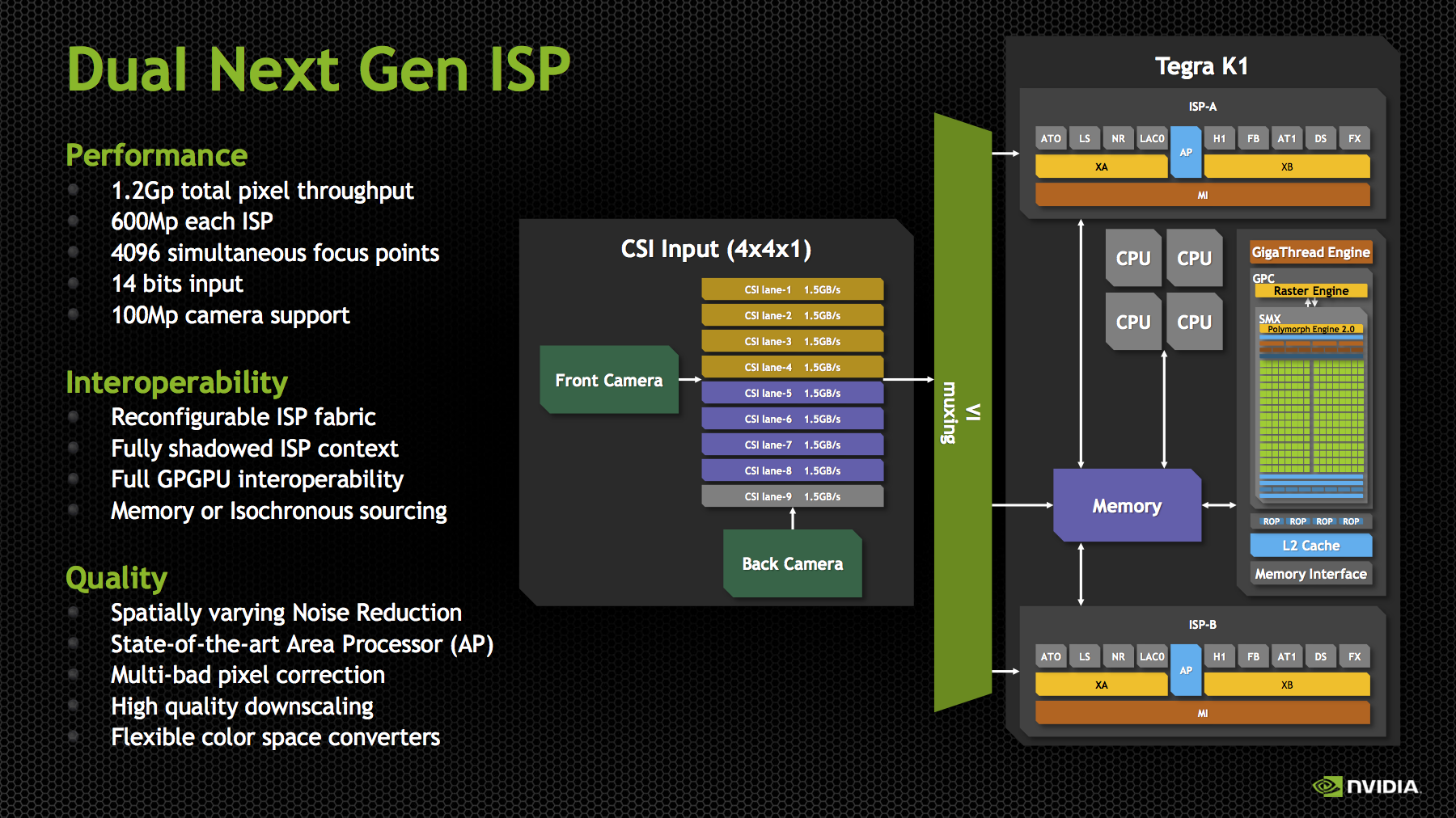
For those not familiar, ISP (Image Signal Processor) handles the imaging pipeline for still photos, video, and performs tasks like Bayer to RGB conversion (demosaicing), 3A (Autofocus, Auto Exposure, Auto white balance), noise reduction, lens correction, and so on. Although NVIDIA has always included an ISP onboard, I couldn’t shake the feeling that still imaging performance could’ve been better, especially in the few cases that allowed direct comparison (HTC One X). With Tegra K1, there’s more die area dedicated to ISP than in the past, and there are two of them to support the kind of dual camera applications that have quickly become popular.
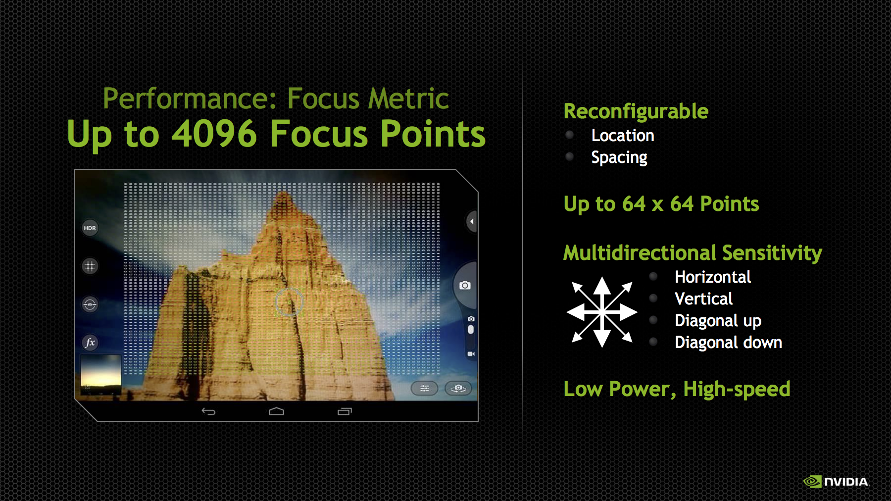
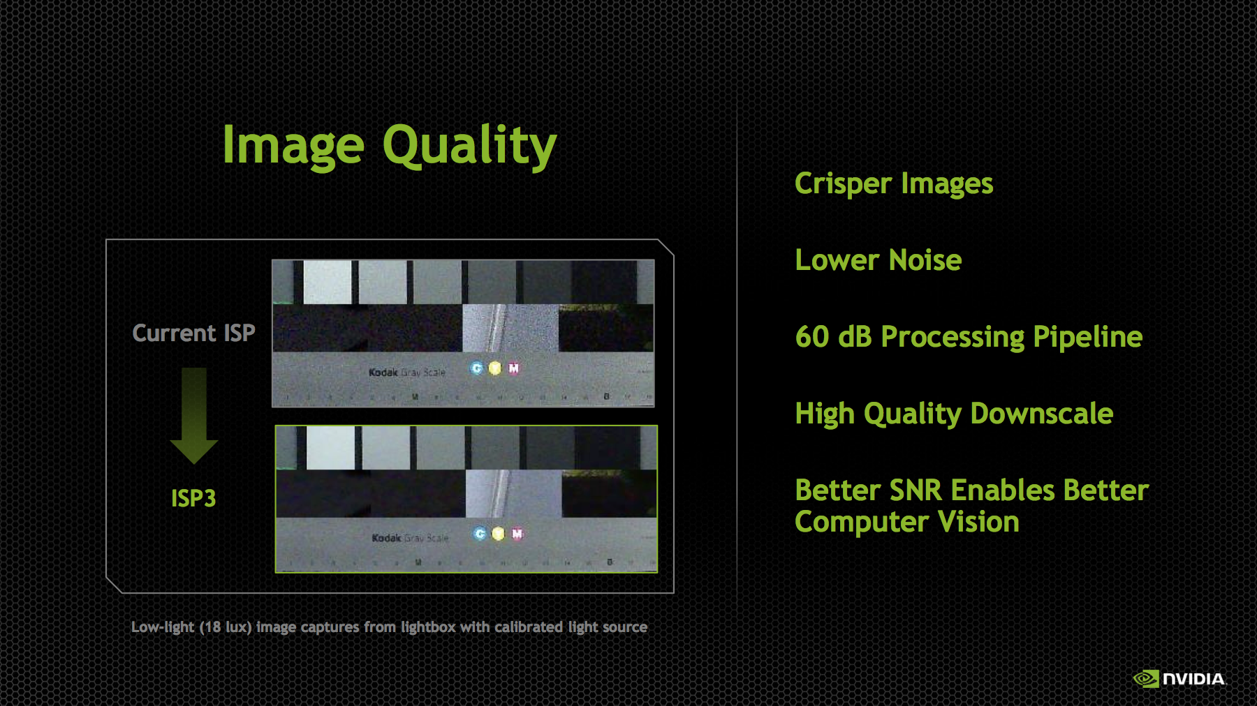
Tegra K1 includes the third generation of NVIDIA’s ISP, capable of processing 600 MP/s on each ISP with 14 bit input, and support for up to 100 MP cameras. There are two of them, so NVIDIA quotes the total pixel throughput as up to 1.2 Gp/s. This is dramatically increased from Tegra 4, which supported up to 400 Mp/s at 10 bits per pixel. In addition the K1’s ISP now supports up to 4096 focus points, a 64x64 array, for its autofocus routine. The ISP also has better noise reduction, and local tone mapping, a feature we’ve also seen become popular for combining parts of images and recovering some of the dynamic range lost with ever shrinking pixel sizes.
Tegra K1 retains compatibility with the Chimera 1.0 features that we just saw in the Tegra Note 7, like object tracking, always-on HDR, slow motion capture, and full resolution burst, and adds more. NVIDIA has kept the Chimera brand for the K1 SoC, calling it Chimera 2.0, and envisions this architecture enabling things like better temporal pixel binning (combining 8 exposures from the CMOS to drive noise down further), faster panorama, video stabilization, and even better live preview with effects applied. The high level of Chimera seems to be the same – kernels that either run on the CPU, or on the GPU (ostensibly in CUDA this time) before or after the ISP and in a variety of image spaces (Bayer or RGB depending).
On the video side, Tegra K1 continues to support 2160p30 (4K or UHD video at 30FPS) encode and decode. Broken down another way, H.264 High Profile Level 5.1 decode and 4K H.264 High Profile 4.2 encode. The fact that there’s a Kepler next door made me suspect that NVENC was used for most of these tasks, but it turns out that NVIDIA still has discrete blocks for video encode of H.264, VP8, VC1, and others. These are the same video encode and decode blocks as what were used in Tegra 4, but with some further optimizations for power and efficiency. The Tegra K1 platform includes support for H.265 video decode as well, but this isn’t accelerated fully in hardware, rather the decode is split across NVENC and CPU.
NVIDIA showed off a K1 reference board doing 4Kp30 H.264 decode on an attached display, I didn’t notice any dropped frames. Of course that’s a given considering we saw the same thing on Tegra 4, but it’s still worth noting that the SoC is capable of driving 4K/UHD displays over eDP 1.4, LVDS and HDMI 1.4b.
The full GPIO breakdown for Tegra K1 includes essentially all the requisite connectivity you’d expect for a mobile SoC. For USB there’s 3 USB 2.0 ports, and 2 USB 3.0 ports. For storage Tegra K1 supports eMMC up to version 4.5.1, and there’s PCIe x4 which can be configured


88 Comments
View All Comments
jerrylzy - Tuesday, January 7, 2014 - link
Exactly. I don't see Loki726's point of gamers paying extra $ for Double Precision. AMD Cards are generally much cheaper at the same performance level, though at the cost of power consumption.Loki726 - Tuesday, January 7, 2014 - link
I mean compared to a world where AMD decided to rip out the double precision units. There are obviously many (thousands) other factors that do into the efficiency of a GPU.jerrylzy - Tuesday, January 7, 2014 - link
Unfortunately, instead of using VLIW 5, Qualcomm implemented new scalar architecture way back in adreno 320.Loki726 - Tuesday, January 7, 2014 - link
Yep, the have improved on it, but they started with the AMD design. My point was that the Qualcomm GPU is a better comparison point to a Tegra SoC than an AMD desktop part.ddriver - Wednesday, January 8, 2014 - link
The decision to chose Qualcomm in favor of Tegra would be based entirely on the absence of OpenCL support in Tegra. Exclusive cuda? Come on, who would want to invest into writing a parallel accelerated high performance routine that only works on like no more than 5% of the hardware-capable to run it devices? Not me anyway.The mention of the radeon was regarding a completely different point - that nvidia sacks DP performance even where it makes no sense to, and is IMO criminal to do so - the "gain" of such a terrible DP implementation is completely diminished by the loss of potential performance and possibility of accelerating a lot of professional workstation software. And for what, so the only spared parts - the "professional" products can have their ridiculous prices better "justified"? Because it is such a sweet deal to make a product 10% more expensive to make and ask 5000% more money for it.
Which is the reason AMD offers so much more value, while limp and non-competitive in the CPU performance, the place where computation is really needed - professional workstation software can greatly benefit from parallelization, and the much cheaper desktop enthusiast product actually delivers more raw computational power than the identical, but more conservatively clocked fireGL analog. Surely, fireGL still has its perks - ECC, double the memory, but those advantages shine in very rare circumstances, in most of the professional computation demanding software the desktop part is still an incredibly lucrative investment, something you just don't get with nvidia because of what they decided to do the last few years, coincidentally the move to cripple DP performance to 1/24 coincided with the re-pimping of the quadros into the tesla line. I think it is rather obvious that nvidia decided to shamelessly milk the parallel supercomputing professional market, something that will backfire in their face, especially stacking with the downplay-ment of OpenCL in favor of a vendor exclusive API to use the hardware.
Loki726 - Wednesday, January 8, 2014 - link
Agreed with the point about code portability, but that's an entirely different issue. I'd actually take the point further and say that OpenCL is too vendor specific -> it only runs on a few GPUs and has shaky support on mobile. Parallel code should be a library like pthreads, C++ (or pick your favorite language) standard library threads, or MPI. Why program in a new language that is effectively C/C++, except that it isn't?I personally think that if a company artificially inflates the price of specific features like double precision, then they leave themselves open to being undercut by a competitor and they will either be forced to change it or go out of business. As I said, AMD's design choice penalizes gamers, but helps users who want compute features, and NVIDIA's choice benefits gamers, but penalizes desktop users who want the best value for some compute features like double precision.
I have a good understanding of circuit design and VLSI implementation of floating point units and I can say that the area and power overheads of adding in 768 extra double precision units to a Kepler GPU or 896 double precision units to a GCN GPU would be noticeable, even if you merged pairs of single precision units together and shared common logic (which would create scheduling hazards at the uArch level that could further eat into perf, and increase timing pressure during layout).
Take a look at this paper from Mark Horowitz (an expert) that explores power and area tradeoffs in floating point unit design if you don't believe me. It should be easy to verify. http://www.cpe.virginia.edu/grads/pdfs/August2012/... . Look at the area and power comparisons in Table 1, scale them to 28nm, and multiply them by ~1000x (to get up to 1/2 or 1/4 of single precision throughput).
Double precision units are big, and adding a lot of them adds a lot of power and area.
Krysto - Saturday, January 11, 2014 - link
I want to believe OpenCL was left out because they've been trying to squeeze so much in this time-frame already. But since they fully ported everything in one swoop, I still find it hard to believe they didn't omit it on purpose. Hopefully, they'll support OpenCL 2.0 in Maxwell, because OpenCL 2.0 also offers some great parallelism features, which Maxwell could take advantage of.Andromeduck - Wednesday, January 8, 2014 - link
Isn't that what the GTX Titan is for?Jon Tseng - Monday, January 6, 2014 - link
Sounds very interesting. The Q for me though as you allude to at the end is whether they can recruit devs to utilise this. Especially when mobile games are a freemium dominated world the temptation is to code for lowest common denominator/max audience, probably with a Samsung label on it (I'm not complaining - its whats enabled me to run World of Tanks happily on my Bay Trail T100!).World beating GPU tech no use unless people are utilising it. Interesting thought about getting MSFT on board though - I guess the downer is that Windows Phone is a minority sport still, and tablet wise it would have to be Windows RT... :-x
nicolapeluchetti - Monday, January 6, 2014 - link
The processing power might be the same as the X-Box 360-PS 3 but using Direct X doesn't incur in a performance Hit?