The Xbox One - Mini Review & Comparison to Xbox 360/PS4
by Anand Lal Shimpi on November 20, 2013 8:00 AM ESTPerformance - An Update
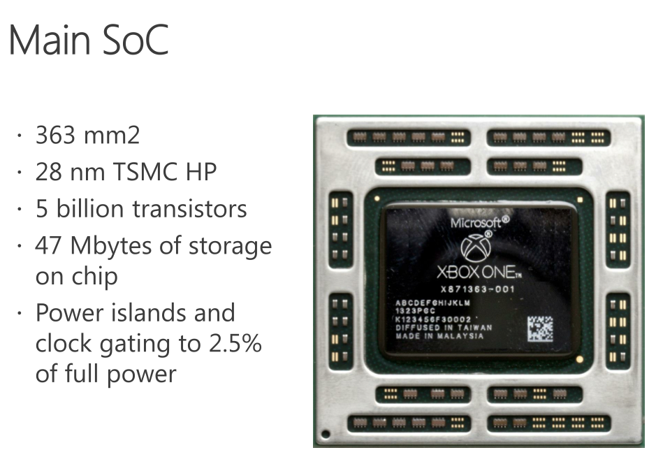
The Chipworks PS4 teardown last week told us a lot about what’s happened between the Xbox One and PlayStation 4 in terms of hardware. It turns out that Microsoft’s silicon budget was actually a little more than Sony’s, at least for the main APU. The Xbox One APU is a 363mm^2 die, compared to 348mm^2 for the PS4’s APU. Both use a similar 8-core Jaguar CPU (2 x quad-core islands), but they feature different implementations of AMD’s Graphics Core Next GPUs. Microsoft elected to implement 12 compute units, two geometry engines and 16 ROPs, while Sony went for 18 CUs, two geometry engines and 32 ROPs. How did Sony manage to fit in more compute and ROP partitions into a smaller die area? By not including any eSRAM on-die.
While both APUs implement a 256-bit wide memory interface, Sony chose to use GDDR5 memory running at a 5.5GHz data rate. Microsoft stuck to more conventionally available DDR3 memory running at less than half the speed (2133MHz data rate). In order to make up for the bandwidth deficit, Microsoft included 32MB of eSRAM on its APU in order to alleviate some of the GPU bandwidth needs. The eSRAM is accessible in 8MB chunks, with a total of 204GB/s of bandwidth offered (102GB/s in each direction) to the memory. The eSRAM is designed for GPU access only, CPU access requires a copy to main memory.
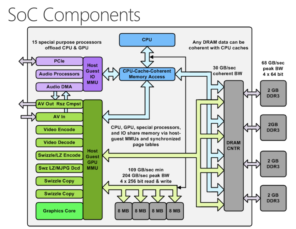
Unlike Intel’s Crystalwell, the eSRAM isn’t a cache - instead it’s mapped to a specific address range in memory. And unlike the embedded DRAM in the Xbox 360, the eSRAM in the One can hold more than just a render target or Z-buffer. Virtually any type of GPU accessible surface/buffer type can now be stored in eSRAM (e.g. z-buffer, G-buffer, stencil buffers, shadow buffer, etc…). Developers could also choose to store things like important textures in this eSRAM as well, there’s nothing that states it needs to be one of these buffers just anything the developer finds important. It’s also possible for a single surface to be split between main memory and eSRAM.
Obviously sticking important buffers and other frequently used data here can definitely reduce demands on the memory interface, which should help Microsoft get by with only having ~68GB/s of system memory bandwidth. Microsoft has claimed publicly that actual bandwidth to the eSRAM is somewhere in the 140 - 150GB/s range, which is likely equal to the effective memory bandwidth (after overhead/efficiency losses) to the PS4’s GDDR5 memory interface. The difference being that you only get that bandwidth to your most frequently used data on the Xbox One. It’s still not clear to me what effective memory bandwidth looks like on the Xbox One, I suspect it’s still a bit lower than on the PS4, but after talking with Ryan Smith (AT’s Senior GPU Editor) I’m now wondering if memory bandwidth isn’t really the issue here.
| Microsoft Xbox One vs. Sony PlayStation 4 Spec comparison | ||||||||||||||
| Xbox 360 | Xbox One | PlayStation 4 | ||||||||||||
| CPU Cores/Threads | 3/6 | 8/8 | 8/8 | |||||||||||
| CPU Frequency | 3.2GHz | 1.75GHz | 1.6GHz | |||||||||||
| CPU µArch | IBM PowerPC | AMD Jaguar | AMD Jaguar | |||||||||||
| Shared L2 Cache | 1MB | 2 x 2MB | 2 x 2MB | |||||||||||
| GPU Cores | 768 | 1152 | ||||||||||||
| GCN Geometry Engines | 2 | 2 | ||||||||||||
| GCN ROPs | 16 | 32 | ||||||||||||
| GPU Frequency | 853MHz | 800MHz | ||||||||||||
| Peak Shader Throughput | 0.24 TFLOPS | 1.31 TFLOPS | 1.84 TFLOPS | |||||||||||
| Embedded Memory | 10MB eDRAM | 32MB eSRAM | - | |||||||||||
| Embedded Memory Bandwidth | 32GB/s | 102GB/s bi-directional (204GB/s total) | - | |||||||||||
| System Memory | 512MB 1400MHz GDDR3 | 8GB 2133MHz DDR3 | 8GB 5500MHz GDDR5 | |||||||||||
| System Memory Bus | 128-bits | 256-bits | 256-bits | |||||||||||
| System Memory Bandwidth | 22.4 GB/s | 68.3 GB/s | 176.0 GB/s | |||||||||||
| Manufacturing Process | 28nm | 28nm | ||||||||||||
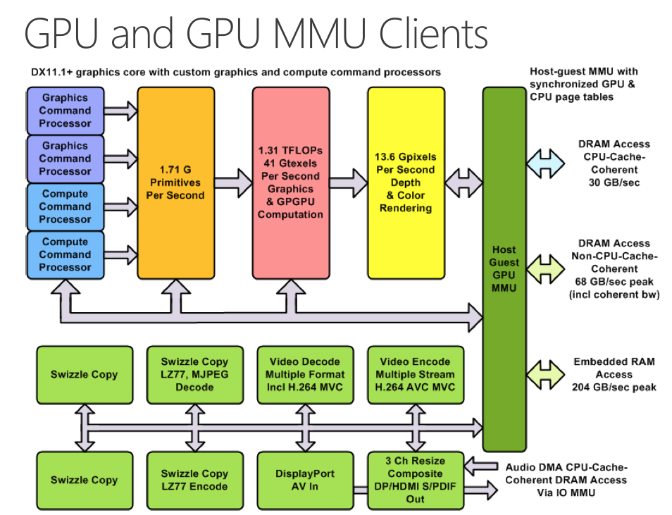
In order to accommodate the eSRAM on die Microsoft not only had to move to a 12 CU GPU configuration, but it’s also only down to 16 ROPs (half of that of the PS4). The ROPs (render outputs/raster operations pipes) are responsible for final pixel output, and at the resolutions these consoles are targeting having 16 ROPs definitely puts the Xbox One as the odd man out in comparison to PC GPUs. Typically AMD’s GPU targeting 1080p come with 32 ROPs, which is where the PS4 is, but the Xbox One ships with half that. The difference in raw shader performance (12 CUs vs 18 CUs) can definitely creep up in games that run more complex lighting routines and other long shader programs on each pixel, but all of the more recent reports of resolution differences between Xbox One and PS4 games at launch are likely the result of being ROP bound on the One. This is probably why Microsoft claimed it saw a bigger increase in realized performance from increasing the GPU clock from 800MHz to 853MHz vs. adding two extra CUs. The ROPs operate at GPU clock, so an increase in GPU clock in a ROP bound scenario would increase performance more than adding more compute hardware.
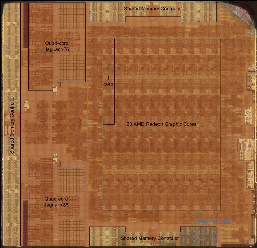 The PS4's APU - Courtesy Chipworks
Microsoft’s admission that the Xbox One dev kits have 14 CUs does make me wonder what the Xbox One die looks like. Chipworks found that the PS4’s APU actually features 20 CUs, despite only exposing 18 to game developers. I suspect those last two are there for defect mitigation/to increase effective yields in the case of bad CUs, I wonder if the same isn’t true for the Xbox One.
At the end of the day Microsoft appears to have ended up with its GPU configuration not for silicon cost reasons, but for platform power/cost and component availability reasons. Sourcing DDR3 is much easier than sourcing high density GDDR5. Sony managed to obviously launch with a ton of GDDR5 just fine, but I can definitely understand why Microsoft would be hesitant to go down that route in the planning stages of Xbox One. To put some numbers in perspective, Sony has shipped 1 million PS4s thus far. That's 16 million GDDR5 chips, or 7.6 Petabytes of RAM. Had both Sony and Microsot tried to do this, I do wonder if GDDR5 supply would've become a problem. That's a ton of RAM in a very short period of time. The only other major consumer of GDDR5 are video cards, and the number of cards sold in the last couple of months that would ever use that RAM is a narrow list.
Microsoft will obviously have an easier time scaling its platform down over the years (eSRAM should shrink nicely at smaller geometry processes), but that’s not a concern to the end user unless Microsoft chooses to aggressively pass along cost savings.


286 Comments
View All Comments
Flunk - Wednesday, November 20, 2013 - link
That's intensely stupid, you're saying that because something is traditional it has to be better. That's a silly argument, not only that it's not even true. The consoles you mentioned all have embedded RAM but all the others from the same generations don't.At this point, arguing that the Xbox One is more powerful or even equivalently powerful is just trolling. The Xbox One and PS4 have very similar hardware, the PS4 just has more GPU units and a higher-performing memory subsystem.
4thetimebeen - Saturday, November 23, 2013 - link
Flunk right now if your saying that the PS4 is more powerful then obviously you base your info in current spec sheet tech and not on the architectural design, but what you don't understand is what's underlining all that new architectural design that has to be learned at the same time it's been used, will only improve exponentially in the future. The PS4 it's straight forward a PC machine with a little mod in the CPU to take better advantage of the GPU but it's pretty much straight forward old design or better said "current architecture GPU design". Which is the reason many say it's easier to program than the Xbox One but right now that "weaker system that you so much swear and affirm is the Xbox One " has a couple game that have been pretty much design for it from the ground up been claim to be the most technical looking advance games on the market right now and you can guess which I'm talking about, that not even that I house 1st party game from Sony can't even compete in looks "KSF". I'm not saying that it's not awesome looking, it is actually but even compared to crisis3 it fails in comparison to that game. So it's suppose to be more easier to develop for, it's suppose to be more powerful and called a super computer, but when looking for that power gap in 1st party games that had the time to invest in its power, the "weaker system" with the hardest to develop architecture show a couple of games that trounces what the "superior machine" was able to show. Hmmm hopefully for you, time will tell and the games will tell the whole story!Owls - Wednesday, November 20, 2013 - link
Calling people names? Haha. How utterly silly for you to say the two different RAM types can be added for a total of 274GB/s. Hey guys it looks like I now have 14400 RPM hard drives now too!smartypnt4 - Wednesday, November 20, 2013 - link
Traditional cache-based architectures rely on all requests being serviced by the cache. This is slightly different, though. I'd be wary of adding both together, as there's no evidence that the SoC is capable of simultaneously servicing requests to both main memory and the eSRAM in parallel. Microsoft's marketing machine adds them together, but the marketing team doesn't know what the hell it's talking about. I'd wait for someone to reverse engineer exactly how this thing works before saying one way or the other, I suppose.It's entirely possible that Microsoft decided to let the eSRAM and main memory be accessed in parallel, but I kind of doubt it. There'd be so little return on the investment required to get that to work properly that it's not really worth the effort. I think it's far more likely that all memory requests get serviced as usual, but if the address is inside a certain range, the access is thrown at the eSRAM instead of the main memory. In this case, it'd be as dumb to add the two together as it would be to add cache bandwidth in a consumer processor like an i5/i7 to the bandwidth from main memory. But I don't know anything for sure, so I guess I can't say you don't get it (since no one currently knows how the memory controller is architected).
hoboville - Thursday, November 21, 2013 - link
smartypnt4's description of eSRAM is very much how typical cache works in a PC, such as L1, L2, L3. It should also be mentioned that L2 cache is almost always SRAM. Invariably, this architecture is just like typical CPU architecture, because that's what AMD Jaguar is. Calls to cache that aren't in the cache address range get forwarded to the SDRAM controller. There is no way Microsoft redesigned the memory controller. That would require changing the base architecture of the APU.Parallel RAM access only exists in systems where there is more than one memory controller or the memory controller is spanned across multiple channels. People who start adding bandwidth together don't understand computer architectures. These APUs are based on existing x86 architectures, with some improvements (look up AMD Trinity). These APUs are not like the previous gen which used IMB POWER cores which are largely different.
rarson - Saturday, November 23, 2013 - link
But Microsoft's chip isn't an APU, it's an SoC. There's silicon on the chip that isn't at all part of the Jaguar architecture. The 32 MB of eSRAM is not L2, Jaguar only supports L2 up to 2 MB per four cores. So it's not "just like a typical CPU architecture."What the hell does Trinity have to do with any of this? Jaguar has nothing to do with Trinity.
4thetimebeen - Saturday, November 23, 2013 - link
Actually if you read and I apologized for up butting in but if you read the digital foundry interview of the Microsoft Xbox One architects that they heavily modified that GPU and it is a DUAL PIPELINE GPU! So your theory is not really far away from the truth!The interview,
http://www.eurogamer.net/articles/digitalfoundry-t...
4thetimebeen - Saturday, November 23, 2013 - link
Plus to add; the idea of adding that DDR3 to the eSRAM kind of acceptable because unlike the PS4 simple straight architecture design like very much the One pool GDDR5 you have 4 modules of DDR3 running at 60- 65gb/s and they each can be used for specific simultaneous request which makes it a lot more advance and more like a future DDR4 way of behaving plus killing that bottleneck people that don't understand, think it has. It's a new tech people and it will take some time to learn its advantages but not hard to program. It's a system design to have less error and be more effective and perform way better than supposedly higher flops GPUS cause it can achieve same performance with less resources! Hope you guys can understand a little and not trying to offend anyone!melgross - Wednesday, November 20, 2013 - link
You really don't understand this at all, do you?fourthletter - Wednesday, November 20, 2013 - link
All the other consoles you mentioned (apart from the PS2) are based on IBM Power PC chips, you are comparing their setup to X86 on the new consoles - silly boy.