Take all of the features of the VP2/97 chipset, double the CPU-to-DRAM Write Buffers, add a full gigabyte of cacheable memory area (which is greater than the 512MB supported by the Pentium II!!!) and AGP support and you get the Apollo VP3 chipset. As the VP2/97 was essentially a combination of the Intel HX and TX chipsets, the VP3 is a combination of the VIA VP2 and the Intel 440LX chipsets. Although the performance of the VP3 has yet to be proven, it will soon by FIC with the release of their PA-2012, the very first Socket-7 AGP Motherboard. VIA has a huge hit on their hands with the combination of the success of the VP2/97 and the imminent success of the VP3 chipset.
Unfortunately there are two significant "let downs" the VP3 chipset leaves us with. The first isn't all that prominent, just that the VP3 doesn't support BEDO DRAM like its predecessors the VP2 and VPX did. Its support for SDRAM as well as DDR-SDRAM does compensate for that shortcoming so it really isn't a huge problem for most users. The big letdown is the lack of a 100MHz bus speed support natively with the VP3 chipset, we will unfortunately have to wait for the next stop in VIA's travels for 100MHz bus speed support with the MVP3 (Mobile VP3).
| VIA VT82C Apollo VP3 Chipset | ||
| Common Name | Apollo VP3 | |
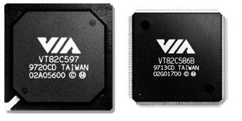
| Chipset Packaging | Number of chips | 2 (VT82C597 System Controller, VT82C586B PCI-to-ISA Bridge) |
| Packaging Type | 1 x 472-pin BGA; 1 x 208-pin QFP | |
| CPU Support | Number of CPUs | 1 |
| AMD CPUs Supported | K5, K6 | |
| Cyrix CPUs Supported | 6x86 (M1), 6x86MX (M2) w/ Linear Burst Mode | |
| Intel CPUs Supported | Pentium, Pentium MMX | |
| Cache | Type | Synchronous Pipeline Burst Cache |
| Maximum Supported Size | 2048KB | |
| Maximum Cacheable DRAM Area | 1GB | |
| Memory | Maximum DRAM Supported | 1GB |
| BEDO DRAM Read Timings (66MHz) | N/A | |
| EDO DRAM Read Timings (66MHz) | 5-2-2-2 | |
| FPM DRAM Read Timings (66MHz) | 5-3-3-3 | |
| SDRAM Read Timings (66MHz) | 3-1-1-1 | |
| Data Path to Memory | 64-bits | |
| ECC Support | Yes | |
| Hard Disk Controller | Chip | VIA BMIDE Controller (VT82C586B) |
| Busmastering Support | Yes | |
| UltraDMA Support | Yes | |
| Max. Theoretical Transfer Rate | PIO Mode 5/DMA Mode 3 (33.3MB/S) | |
| PCI Interface | Supported PCI Bus Speeds | 25, 30, 33 MHz |
| Concurrent PCI | Yes | |
| Async. PCI Bus Speed | No | |
| PCI Specification | 2.0 (66 MHz max.) | |
| Power Management | PC97 Compliance | Yes |
| Suspend to Disk | Yes | |
| HDD Power Down | Yes | |
| Modem Wakeup | Yes | |
| System Suspend | Yes | |
| Video | AGP Support | Yes |
| Unified Memory Architecture | No | |
| Peripheral Support | USB Support | Yes |
| Plug and Play Port | Yes | |
| Write Buffers | CPU-to-DRAM | 32 QWords |
| CPU-to-PCI | 6 DWords | |
| PCI-to-DRAM | 48 DWords | |
| Officially Supported Bus Speeds | 50, 60, 66 MHz | |
| Unofficially Achieved Bus Speeds | Unknown | |


4 Comments
View All Comments