Intel's Xeon E5-2600 V2: 12-core Ivy Bridge EP for Servers
by Johan De Gelas on September 17, 2013 12:00 AM ESTWhat Has Improved?
Ivy Bridge is what Intel calls a tick+, a transition to the latest 22nm process technology (the famous P1270 process) with minor architectural optimizations compared to predecessor Sandy Bridge (described in detail by Anand here):
- Divider is twice as fast
- MOVs take no execution slots
- Improved prefetchers
- Improved shift/rotate and split/Load
- Buffers are dynamically allocated to threads (not statically split in two parts for each thread)
Given the changes, we should not expect a major jump in single-threaded performance. Anand made a very interesting Intel CPU generational comparison in his Haswell review, showing the IPC improvements of the Ivy Bridge core are very modest. Clock for clock, the Ivy Bridge architecture performed:
- 5% better in 7-zip (single-threaded test, integer, low IPC)
- 8% better in Cinebench (single-threaded test, mostly FP, high IPC)
- 6% better in compiling (multi-threaded, mostly integer, high IPC)
So the Ivy Bridge core improvements are pretty small, but they are measureable over very different kinds of workloads.
The core architecture improvements might be very modest, but that does not mean that the new Xeon E5-2600 V2 series will show insignificant improvements over the previous Xeon E5-2600. The largest improvement comes of course from the P1270 process: 22nm tri-gate (instead of 32nm planar) transistors. Discussing the actual quality of Intel process technology is beyond our expertise, but the results are tangible:
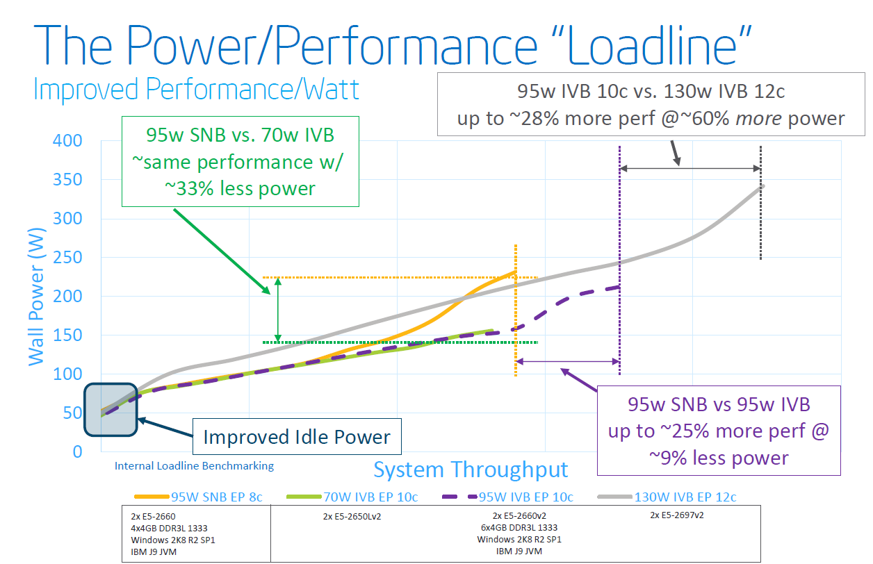
Focus on the purple text: within the same power envelope, the Ivy Bridge Xeon is capable of delivering 25% more performance while still consuming less power. In other words, the P1270 process allowed Intel to increase the number of cores and/or clock speed significantly. This can be easily demonstrated by looking at the high-end cores. An octal-core Xeon E5-2680 came with a TDP of 130W and ran at 2.7GHz. The E5-2697 runs at the same clock speed and has the same TDP label, but comes with four extra cores.
Virtualization Improvements
Each new generation of Xeon has reduced the amount of cycles required for a VMexit or a VMentry, but another way to reduce hardware virtualization overhead is to avoid VMexits all together. One of the major causes of VMexits (and thus also VMentries) are interrupts. With external interrupts, the guest OS has to check which interrupt has the priority and it does this by checking the APIC Task Priority Register (TPR). Intel already introduced an optimization for external interrupts in the Xeon 7400 series (back in 2008) with the Intel VT FlexPriority. By making sure a virtual copy of the APIC TPR exists, the guest OS is capable of reading out that register without a VMexit to the hypervisor.
The Ivy Bridge core is now capable of eliminating the VMexits due to "internal" interrupts, interrupts that originate from within the guest OS (for example inter-vCPU interrupts and timers). The virtual processor will then need to access the APIC registers, which will require a VMexit. Apparantly, the current Virtual Machine Monitors do not handle this very well, as they need somewhere between 2000 to 7000 cycles per exit, which is high compared to other exits.
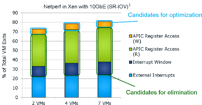
The solution is the Advanced Programmable Interrupt Controller virtualization (APICv). The new Xeon has microcode that can be read by the Guest OS without any VMexit, though writing still causes an exit. Some tests inside the Intel labs show up to 10% better performance.
Related to this, Sandy Bridge introduced support for large pages in VT-d (faster DMA for I/O, chipset translates virtual addresses to physical), but in fact still fractioned large pages into 4KB pages. Ivy Bridge fully supports large pages in VT-d.
Only Xen 4.3 (July 2013) and KVM 1.4 (Spring 2013) support these new features. Both VMware and Microsoft are working on it, but the latest documents about vSphere 5.5 do not mention anything about APICv. AMD is working on an alternative called Advanced Virtual Interrupt Controller (AVIC). We found AVIC inside the AMD64 programmer's manual at page 504, but it is not clear which Opterons will support it (Warsaw?).


70 Comments
View All Comments
Kevin G - Tuesday, September 17, 2013 - link
I'd be careful about using Java benchmarks on those SPARC chips for an overall comparison. The results on the SPARC side are often broken.x86 for many years has been ahead of SPARC. Only with the most recent chips has Oracle produced a very performance competitive chip.
The only other architecture that out runs Intel's best x86 chips is the POWER7/POWER7+. When the POWER8 ships, it is expected to be faster still.
Brutalizer - Thursday, September 19, 2013 - link
@Kevin G"...The results on the SPARC side are often broken..."
What do you mean with that? The Oracle benchmarks are official and anyone can see how they did it. Regarding the SPARC T5 performance, it is very fast, typically more than twice as fast as Xeon cpus. Just look at the official, accepted benchmarks on the site I linked to.
Kevin G - Friday, September 20, 2013 - link
@BrutalizerThere is a SPEC subtest whose result on SPARC is radically higher than other platforms. The weight of this one test affects the overall score. It has been a few years since I read up about this and SPARC as a platform has genuinely become performance competitive again.
Phil_Oracle - Friday, February 21, 2014 - link
Are you talking about libquantum?http://www.spec.org/cpu2006/Docs/462.libquantum.ht...
I believe IBM is the worst culprit on this subtest, showing a significant difference between base and peak. More so than any other vendor.
http://www.spec.org/cpu2006/results/res2012q4/cpu2...
But today, I believe all vendors have figured out how to improvise (cheat) on this test, even Xeon based.
http://www.spec.org/cpu2006/results/res2014q1/cpu2...
That’s why I believe SPEC CPU2006 is outdated and needs replacing and suggest looking at more realistic, recent (dal world) benchmarks like SPECjbb2013, SPECjEnterprise2010 or even TPC-H.
Phil_Oracle - Friday, February 21, 2014 - link
x86 was clearly ahead of SPARC till about SPARC T4 timeframe when Oracle took over R&D on SPARC. SPARC T4 allowed Oracle to equalize the playing field, especially in areas like database where the SPARC T4 really shines and shows considering many of the world record benchmarks that where released. When SPARC T5 came out last year, it increased performance by 2.4x, clobbering practically every other CPU out there. Today, you'll be hard pressed to find a real world benchmark, ones that are fully audited, where SPARC T5 is not in a leadership position, whether java based like SPECjbb2013 or SPECjEnterprise2010 or database like TPC-C or TPC-H.psyq321 - Tuesday, September 17, 2013 - link
I know that EX will be using the (scalable) memory buffer, which is probably the main reason for the separate pin-out. I guess they could still keep both memory controllers in, and fuse the appropriate one depending if it is an EX or EP SKU, if this would still make sense from a production perspective.Kevin G - Tuesday, September 17, 2013 - link
It wouldn't make much sense as the EX line up moves the DDR3 physical interface off to the buffer chip. There is a good chunk of die space used for the 256 bit wide memory interface in the EP line. Going the serial route, the EX line is essentially doubling the memory bandwidth while using the same number of IO pins (though at the cost of latency).The number of PCIe lanes and QPI links also changes between the EP and EX line up. The EP has 40 PCIe lanes where as the EX has 32. There are 4 QPI links on the EX line up making them ideal for 4 and 8 socket systems were as the EP line has 2 QPI links good for dual or a poor quad socket configuration.
psyq321 - Wednesday, September 18, 2013 - link
Hmm, this source: http://www.3dcenter.org/news/intel-stellt-ivy-brid...Claims that HCC is 12-15 core design. They also have a die-shot of a 15 core variant.
Kevin G - Thursday, September 19, 2013 - link
I'll 1-up you: Intel technical reference manuals (PDF).http://www.intel.de/content/dam/www/public/us/en/d...
http://www.intel.de/content/dam/www/public/us/en/d...
It does appear to be 15 core judging from the mask in the CSR_DESIRED_CORES register.
However, there is not indication that the die supports serial memory links to a buffer chip or >3 QPI links that an EX chip would have.
psyq321 - Thursday, September 19, 2013 - link
Well, I guess without Intel openly saying or somebody laser-cutting the die it would not be possible to know exactly is it a shared die between HCC EP and EX.However, there are lots of "hints" that the B-package Ivy Bridge EP hide more cores, like the ones you linked. If it is the case, it is really a shame that Intel did not enable all cores in the EP line. There would still be lots of places for differentiation between the EX and EP lines, since EX anyway contains RAS features without which the target enterprise customers would probably not even consider EP, even if it had the same number of cores.
Also, Ivy EX will have some really high TDP parts.