Samsung’s V-NAND: Hitting the Reset Button on NAND Scaling
by Anand Lal Shimpi on August 21, 2013 2:50 AM EST
SSD pricing has come down tremendously since Intel’s X25-M hit the scene in 2008. Back then we were talking about 80GB for around $600, while today Micron and Samsung will sell you a 1TB SSD for the same price. Moore’s Law drove this scaling in capacity. Smaller transistors paved the way for higher density NAND in the same die area, and increasing volumes helped to keep the fabs full.
Although scaling transistor size helped address the cost-per-bit problem, it created a new one: decreasing endurance and performance. Just looking at what’s happened to IMFT NAND over the past few generations gives us an idea of what we’re dealing with:
| Micron NAND Evolution | ||||||||||||
| 50nm | 34nm | 25nm | 20nm | 20nm | 16nm | |||||||
| Single Die Max Capacity | 16Gbit | 32Gbit | 64Gbit | 64Gbit | 128Gbit | 128Gbit | ||||||
| Program Page (typical) | 900 µs | 1200 µs | 1300 µs | 1300 µs | 1600 µs | ? | ||||||
| Rated Program/Erase Cycles | 10000 | 5000 | 3000 | 3000 | 3000 | ~3000 | ||||||
Both endurance and performance trend downwards. Modern SSDs deal with the endurance problem by implementing sophisticated error checking/correction, and the performance problem is masked by exploiting parallelism as best as possible.
The root cause is basic physics. To store 2 bits per cell in present day MLC NAND, we’re talking about counting a couple dozen electrons. Go to 3 bits per cell (TLC NAND) and the difference between levels shrinks further. Scale down to 14/15/16nm NAND and everything gets more difficult. We’re heading towards a situation where the difference between levels in a NAND cell are a matter of a handful of electrons.

Measuring such subtle differences in stored charge is difficult, especially when NAND cells continue to shrink and are packed very tightly together. Interference between the cells becomes a much bigger concern below 20nm. Back at 50nm these sorts of issues were easy to mitigate with decent controllers and good quality NAND. Now we’re seeing more sophisticated ECC and DSP-like work being done by the controller in order to get accurate data in/out of the drive.
Scaling of traditional NAND via smaller manufacturing processes will come to an end. I’ve heard estimates saying we’ll see one or two more shrinks before it becomes unfeasible to scale cell size any further. The question then becomes: what’s next?
Last week Samsung gave their answer: V-NAND, a 3D NAND leveraging charge trap flash technology.
How it Works
Rather than increasing density by shrinking cell size, Samsung’s V-NAND takes a few steps back in process technology and instead stacks multiple layers of NAND cells on top of one another.
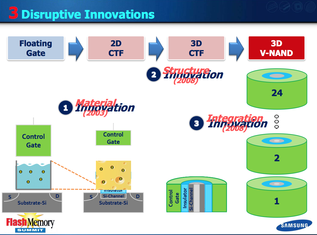
The change isn’t so simple. I’ve used the floating gate transistor diagram in many of our big SSD articles in the past, but that cell design doesn’t apply to V-NAND. In the floating gate MOSFET, electrons are stored on the gate itself - a conductor. Defects in the transistor (e.g. from repeated writes) can cause a short between the gate and channel, depleting any stored charge in the gate. If the gate is no longer able to reliably store a charge, then the cell is bad and can no longer be written to. Ultimately this is what happens when you wear out an SSD.
With V-NAND, Samsung abandons the floating gate MOSFET and instead turns to its own Charge Trap Flash (CTF) design. An individual cell looks quite similar, but charge is stored on an insulating layer instead of a conductor. This seemingly small change comes with a bunch of benefits, including higher endurance and a reduction in overall cell size. That’s just part of the story though.
V-NAND takes this CTF architecture, and reorganizes it into a non-planar design. The insulator surrounds the channel, and the control gate surrounds it. The 3D/non-planar design increases the physical area that can hold a charge, which in turn improves performance and endurance.
The final piece of the V-NAND puzzle is to stack multiple layers of these 3D CTF NAND cells. Since Samsung is building density vertically, there’s not as much pressure to shrink transistor sizes. With relaxed planar space constraints, Samsung turned to an older manufacturing process (30nm class, so somewhere between 30 and 39nm) as the basis of V-NAND.
By going with an older process, Samsung inherently benefits from higher endurance and interference between cells is less of an issue. Combine those benefits with the inherent endurance advantages of CTF and you end up with a very reliable solution. Whereas present day 19/20nm 2-bit-per-cell MLC NAND is good for around 3000 program/erase cycles, Samsung’s 30nm-class V-NAND could withstand over 10x that (35K p/e cycles).
The move to an older process node doesn’t even come at a reduction in density thanks to just how high Samsung can stack its V-NAND. In its announcement last week, Samsung introduced a first generation 128Gbit MLC V-NAND solution with 24 layers. The 128Gbit device delivers 2x the density in the same physical space as a 19/20nm 64Gbit device, or roughly equivalent density to a traditional 128Gbit planar device at 15nm - the obvious benefit being better endurance, and performance.
Since we’re dealing with physically larger NAND cells that are also less susceptible to certain types of interference, program times are lower - meaning that performance is higher. With fewer retries required for all reads/writes, overall power consumption can be lower as well. At the end of the day, it’s just a better solution.
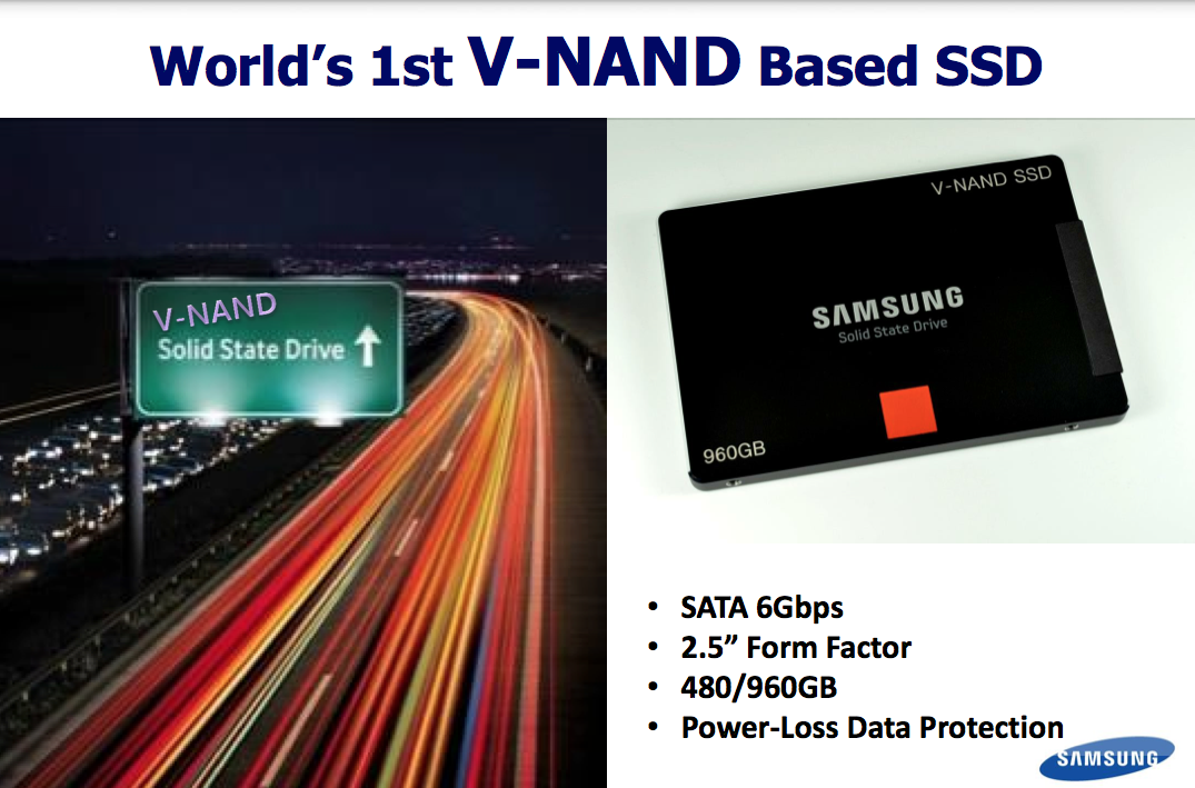
Samsung went one step further and announced that it was sampling an enterprise SSD built around V-NAND to key customers. Since V-NAND is presently only available in a 128Gbit density, capacities aren't anything earth shattering but I suspect that'll change soon enough. It’s too early to talk about pricing and availability unfortunately.
V-NAND is the future for Samsung. We’ll see V-NAND in appear in enterprise, client and even mobile (phones/tablets). There will likely be a period of overlap as Samsung transitions to V-NAND, but expect to see that transition begin next year across multiple markets.
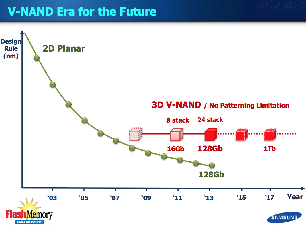
A 128Gbit device is nice, but that’s not the end of the road. Samsung is predicting it’ll be able to build a 1Tb device by 2017, showcasing just how much scaling it can get out of 3D NAND. Samsung could theoretically also move to a smaller process node to further increase density, although ultimately that will run into the same limitations we’re facing today with traditional, planar NAND. The initial design only stores two bits per cell, but if need be Samsung could also move to a TLC V-NAND.
What about the rest of the present day NAND players? I suspect those that don’t move to CTF and/or 3D NAND will instead have their sights set on a bigger departure from NAND: some form of resistive RAM. The potential performance gains there are even higher, and you can also deploy a vertically stacked solution to gain density.
The good news is that it looks like we’re going to have some great options that will enable continued improvements in SSD density, cost and performance.


44 Comments
View All Comments
I_M - Wednesday, January 1, 2014 - link
So where are those 480GB and 960GB Samsung V-NAND SSD that are supposed to be manufactured from Aug 2013?Looks like complete vaporware as of 1/1/2014. - not even part numbers could be found on Samsung websites.
MarcSP - Friday, March 28, 2014 - link
Now we know the real meaning of that V: Vapor-NAND :-PMarcSP - Friday, March 28, 2014 - link
And if we flip vertically that V, it looks very much like "A-NAND":OMG, it was just a joke from Samsung to mess with Anand Shimp and Anandtech.com!
doggface - Sunday, February 14, 2016 - link
It is now 2016... And we are into 2tb.. So ... They kind of won this one. So much for your snarky comment.