Samsung’s 3D Vertical NAND Set to Improve NAND Densities
by Jarred Walton on August 6, 2013 6:12 PM EST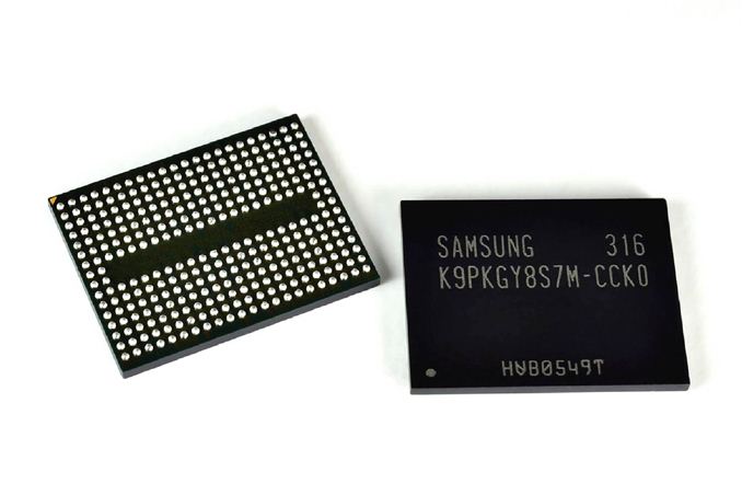
Ars Technica has posted information on Samsung’s new 3D Vertical NAND technology, and it promises to boost densities for SSDs and other similar devices dramatically. Samsung announced last night that they have begun mass production of the devices.
Using up to 24 vertical NAND elements, Samsung predicts that they will be able to scale up to 1Tb per individual NAND chip. It’s not clear exactly how large the initial chips will be, but with conventional 19nm NAND currently shipping in 128Gb capacities we’d expect at least two to four times as much storage per chip. That means using current SSD standards of eight channels of NAND we’d see capacities for “commodity” SSDs move from 128GB to 256GB or even 512GB, and with four NAND die per package we could easily hit 2TB SSDs. The days of needing a secondary storage device with a hard drive could be quickly coming to a close depending on the timing and pricing.
There’s a second technology also coming into play with V-NAND that addresses concerns with reliability and longevity of NAND. Rather than storing charge in a set of floating gate transistors, with voltage levels corresponding to either 0/1 (SLC), 00/01/10/11 (MLC), or 000/001/010/011/100/101/110/111 (TLC), V-NAND will use Charge Trap Flash (CTF). Samsung states, “With Samsung's CTF-based NAND flash architecture, an electric charge is temporarily placed in a holding chamber of the non-conductive layer of flash that is composed of silicon nitride (SiN), instead of using a floating gate to prevent interference between neighboring cells.” Samsung claims that at a minimum CTF will have at least 2x the lifespan of floating gate NAND, and potentially as much as a 10x increase. Write performance is also doubled relative to conventional 10nm-class floating gate NAND.
Sadly, there’s no specific word on availability or pricing right now, and historically with V-NAND just entering mass production we’re likely a year or more away from production SSDs using the technology. Samsung is obviously a major player in both the NAND and SSD markets, so Samsung SSDs using V-NAND are inevitable, but testing and validation will certainly require some time. Hopefully this all comes sooner rather than later, though, as the potential to ditch conventional storage and get improved performance and reliability compared to current NAND seems like the perfect storm needed to end our reliance on slow, spinning platters.
Source: Ars Technica


33 Comments
View All Comments
Mondozai - Wednesday, August 7, 2013 - link
Tablets, possibly. Phones? Heh.Mondozai - Wednesday, August 7, 2013 - link
By the way, does this, in any significant way, affect thickness of a slim smartphone or is the stacking so neglible that it won't matter? Enlightenment, please.JarredWalton - Wednesday, August 7, 2013 - link
My understanding is that the stacking only adds a very small amount to the z-height of one chip, and it should be easy enough to accommodate. I believe some of the upcoming CPUs (Broadwell or Skylake) are expected to do something similar with stacked DRAM vs. stacked NAND. If each layer of NAND adds even 1000nm to the total height of the chip (which would be pretty extreme I would think -- 50-100nm would seem a more likely target), 24 layers would increase the height of the chip by 24um, or 0.024mm.Jaybus - Thursday, August 8, 2013 - link
Negligible and won't affect it.beginner99 - Wednesday, August 7, 2013 - link
If true IMHO this could be one of the most disruptive inventions in the tech sector lately. The only problem I see is a lot higher price compared to normal NAND and hence less of an actual benefit. And then my media files are perfectly fine on a slow ass green drive. So if this new SSD would only cost double, well it's still a lot more given one does not need the performance.althaz - Wednesday, August 7, 2013 - link
I wouldn't bother for my media drives at double the price, but I sure as hell would for my games drive!dali71 - Wednesday, August 7, 2013 - link
RRAM will laugh at NAND's puny capacity and speed:http://www.engadget.com/2013/08/06/crossbar-rram/
klmccaughey - Wednesday, August 7, 2013 - link
Been hearing about this for years now and it's still pie in the sky - when I see a finished product at a reasonable price from RRAM I will believe it.MrSpadge - Wednesday, August 7, 2013 - link
To be fair, Crossbar showed much more than HP ever did - a taped out chip produced at 25 nm and being significantly smaller than NAND at this node. That's something companies can actually use and test - and if it's as good as they someone will start building devices out of it. At least OCZ, they're always up fancy new stuff, despite taking huge risks.klmccaughey - Wednesday, August 7, 2013 - link
Also, I remember at the time it had terrible endurance. Hopefully this has been solved.