The ARM Diaries, Part 2: Understanding the Cortex A12
by Anand Lal Shimpi on July 17, 2013 12:30 PM EST- Posted in
- CPUs
- Arm
- SoCs
- Cortex A12
Introduction to Cortex A12 & The Front End
At a high level ARM’s Cortex A12 is a dual-issue, out-of-order microarchitecture with integrated L2 cache and multi-core capable.
The Cortex A12 team all previously worked on Cortex A9. ARM views the resulting design as not being a derivative of Cortex A9, but clearly inspired by it. At a high level, Cortex A12 features a 10 - 12 stage integer pipeline - a lengthening of Cortex A9’s 8 - 11 stage pipeline. The architecture is still 2-wide out-of-order, but unlike Cortex A9 the new tweener is fully out of order including load/store (within reason) and FP/NEON.

Cortex A12 retains feature and ISA compatibility with ARM’s Cortex A7 and A15, making it the new middle child in the updated microprocessor family. All three parts support 40-bit physical addressing, the same 128-bit AXI4 bus interface and the same 32-bit ARM-v7A instruction set (NEON is standard on Cortex A12). The Cortex A12 is so compatible with A7 and A15 that it’ll eventually be offered in a big.LITTLE configuration with a cluster of Cortex A7 cores (initial versions lack the coherent interface required for big.LITTLE).
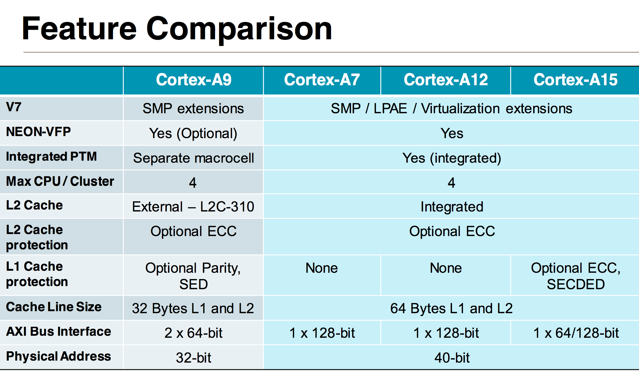
In the Cortex A9, ARM had a decoupled L2 cache that required some OS awareness. The Cortex A12 design moves to a fully integrated L2, similar to the A7/A15. The L2 cache operates on its own voltage and frequency planes, although the latter can be in sync with the CPU cores if desired. The L2 cache is shared among up to four cores. Larger core count configurations are supported through replication of quad-core clusters.
The L1 instruction cache is 4-way set associative and configurable in size (32KB or 64KB). The cache line size in Cortex A12 was increased to 64 bytes (from 32B in Cortex A9) to better align with DDR memory controllers as well as the Cortex A7 and A15 designs. Similar to Cortex A9 there’s a fully associative instruction micro TLB and unified main TLB, although I’m not sure if/how the sizes of those two structures have changed.
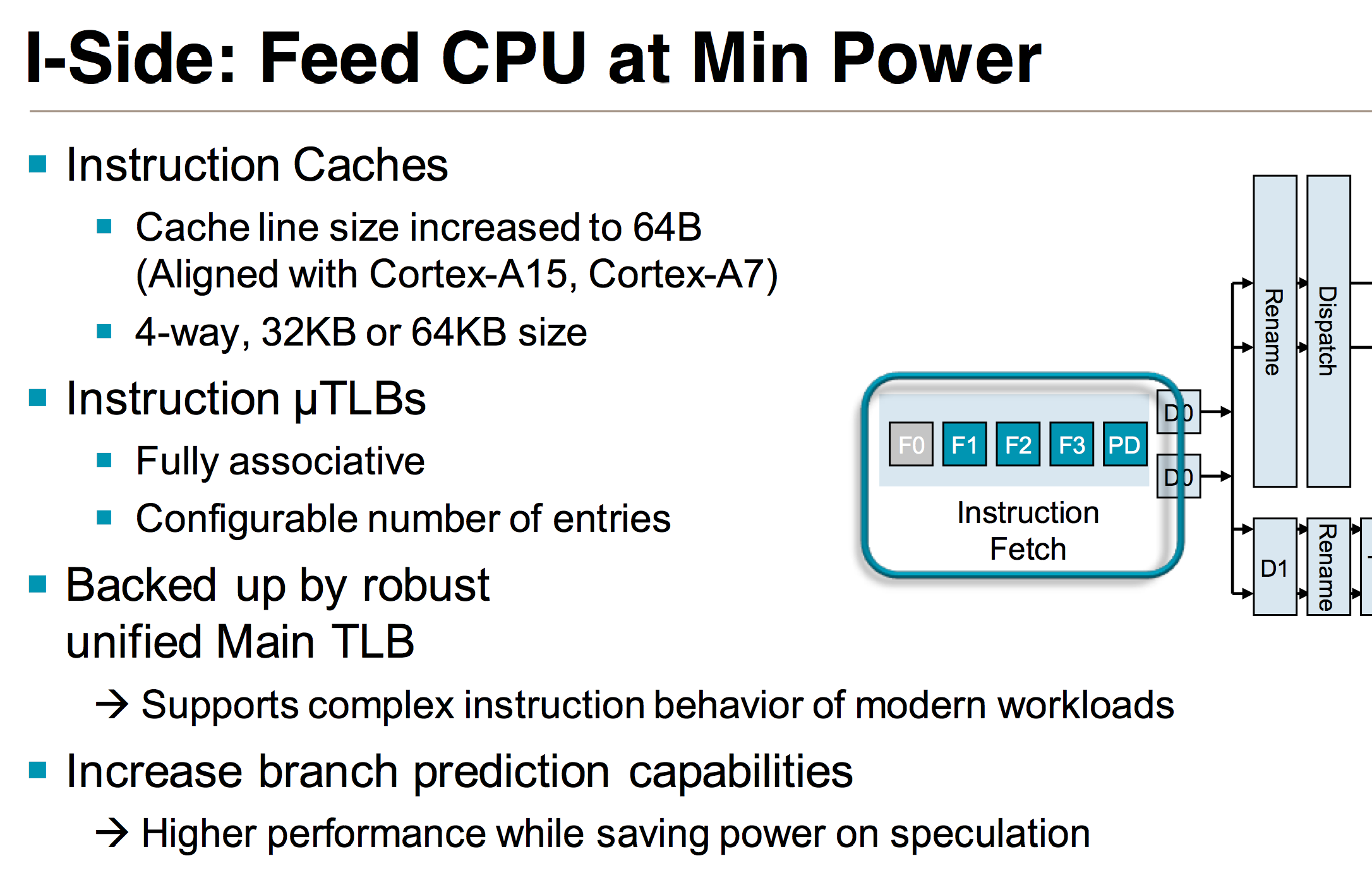
The branch predictor was significantly improved over Cortex A9. Apparently in the design of the Cortex A12, ARM underestimated its overall performance and ended up speccing it out with too weak of a branch predictor. About three months ago ARM realized its mistake and was left with the difficult situation of either shipping a less efficient design, or quickly finding a suitable branch predictor. The Cortex A12 team went through the company looking for a designed predictor it could use, eventually finding one in the Cortex A53. The A53’s predictor got pulled into the Cortex A12 and with some minor modifications will be what the design ships with. Improved branch prediction obviously improves power efficiency as well as performance.


65 Comments
View All Comments
wumpus - Friday, July 19, 2013 - link
And I didn't see anyway for 32bit ARM to access more than 3G. Maybe there is, but the PAE-style mechanism that allowed each process to access 4G of ram (well 2-3G of user space and 2-1G of OS space). It looks like each process sees 32 bit MMU tags meaning no way to access the whole RAM. Again, somewhere in there they might have an unholy kludge, but I suspect that they are more than willing to do things the [PAE] intel way [not the 286 way that Microsoft forced everyone to support a decade after it was consigned to the junkyard].wumpus - Friday, July 19, 2013 - link
So how does one process access more than 4G (3G if Linux, likely less else where)? There is a reason nobody uses 32 bit chips. If you really looked up the datasheets, the *80386* chip could access way more than 64G virtual ram (it didn't have the pins for more than 4G of memory). You could even access it fairly easily in a process, but as far as I know *nobody* ever tried that.Note: Linux 0.x and I think 1.x could both handle 3G per memory process. Maybe not, I know Linus used the 386 segmentation scheme natively on different processes, but I have no idea if the 386 MMU could handle tags that depended on the segmentation scheme (it was quite possible you could either go wild with segments, or use them traditionally and have full MMU operation. I haven't looked at this stupid idea since 1990, when I learned the disaster that is x86.
We use 64 bit chips for a reason. If we didn't need to access memory the size of an integer register, I would strongly suspect that all integer registers would be 16 bits long (note the pentium4 computed integer operations 16 bits at a time, they are notably faster). Using a 64 bit register and 64 bit addressing means that you can access an entire database of arbitrary size (2^63, whatever that is), while using 32 bit machines requires a "networking" OS call to whichever process happens to have that particular datum in memory. It is yet another unholy kludge and the reason that "the only fatal mistake a computer architecture can have is too small a word size".
Wilco1 - Friday, July 19, 2013 - link
You don't need to access more than 3GB per process on a mobile! Mobiles/tablets will have 4GB of RAM, however each process still has it's own 32-bit address space and uses only a portion of the available RAM.There is no need to be so obsessed about 64-bit, you know the the Windows world is still mostly 32-bit 10 years after the introduction of Athlon64... Even Windows 8 still has a 32-bit version. So while there are lots of 64-bit chips around, most run only 32-bit code. My Athlon64 which I retired last year never ever ran 64-bit code during its entire life!
You only really require 64-bit addressing if you have big applications that need more than 3GB per process. Such applications are rare (your database is an example) and they only run on large expensive servers, not on mobiles. So clearly the need for 64-bit is extremely small, and mobiles/tablets will simply use PAE rather than switch to 64-bit for the foreseeable future.
Calinou__ - Saturday, July 20, 2013 - link
64 bit is still a technogy of the future. Not to mention PAE can be quite buggy sometimes, especially when running eg. proprietary drivers.Wolfpup - Thursday, July 25, 2013 - link
The timing on this seems weird. Didn't they know they needed a smaller jump between A9 and A15 years ago? I HOPE it's not really needed by late 2014/2015...I mean I hope by then we're all using A15, and maybe A5x or whatever... Or AMD's low power chips and SIlvermont!