The 2013 MacBook Air Review (13-inch)
by Anand Lal Shimpi on June 24, 2013 12:01 AM ESTA Custom Form Factor PCIe SSD
In the old days, increasing maximum bandwidth supported by your PATA/SATA interface was always ceremonial at first. Hard drives were rarely quick enough to need more than they were given to begin with, and only after generations of platter density increases would you see transfer rate barriers broken. Then came SSDs.
Not only do solid state drives offer amazingly low access latency, but you can hit amazingly high bandwidth figures by striping accesses across multiple NAND Flash die. A 256GB SSD can be made up of 32 independent NAND die, clustered into 8 discrete packages. A good controller will be able to have reads/writes in flight to over half of those die in parallel. The result is a setup that can quickly exceed the maximum bandwidth that SATA can offer. Today that number is roughly 500MB/s for 6Gbps SATA, which even value consumer SSDs are able to hit without trying too hard. Rather than wait for another rev of the SATA spec, SSD controller makers started eyeing native PCIe based controllers as an alternative.
You can view a traditional SSD controller as having two sides: one that talks to the array of NAND flash, and one that talks to the host system’s SATA controller. The SATA side has been limiting max sequential transfers for a while now at roughly 550MB/s. The SATA interface will talk to the host’s SATA interface, which inevitably sits on a PCIe bus. You can remove the middle man by sticking a native PCIe controller on the SSD controller. With SATA out of the way, you can now easily scale bandwidth by simply adding PCIe lanes. The first generation of consumer PCIe SSDs will use PCIe 2.0, since that’s what’s abundant/inexpensive and power efficient on modern platforms. Each PCIe lane is good for 500MB/s, bidirectional (1GB/s total). Apple’s implementation uses two PCIe 2.0 lanes, for a total of 1GB/s of bandwidth in each direction (2GB/s aggregate).
The move to a PCIe 2.0 x2 interface completely eliminates the host side bottleneck. As I pointed out in my initial look at the new MacBook Air, my review sample’s 256GB SSD had no problems delivering almost 800MB/s in peak sequential reads/writes. Do keep in mind that you’ll likely see slower results on the 128GB drive.
Users have spotted both Samsung and SanDisk based PCIe SSDs in the 2013 MacBook Airs. Thankfully Apple doesn’t occlude the controller maker too much in its drive names. An SM prefix denotes Samsung:
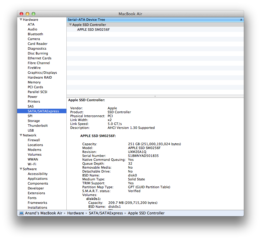
My review sample featured a Samsung controller. There’s very little I know about the new Samsung controller, other than it is a native PCIe solution that still leverages AHCI (this isn't NVMe). Within days of Apple launching the new MBAs, Samsung announced its first consumer PCIe SSD controller: the XP941. I can only assume the XP941 is at least somewhat related to what’s in the new MBA.
The Samsung controller is paired with a 512MB DDR3 DRAM and 8 Samsung 10nm-class (10nm - 20nm process node) MLC NAND devices.
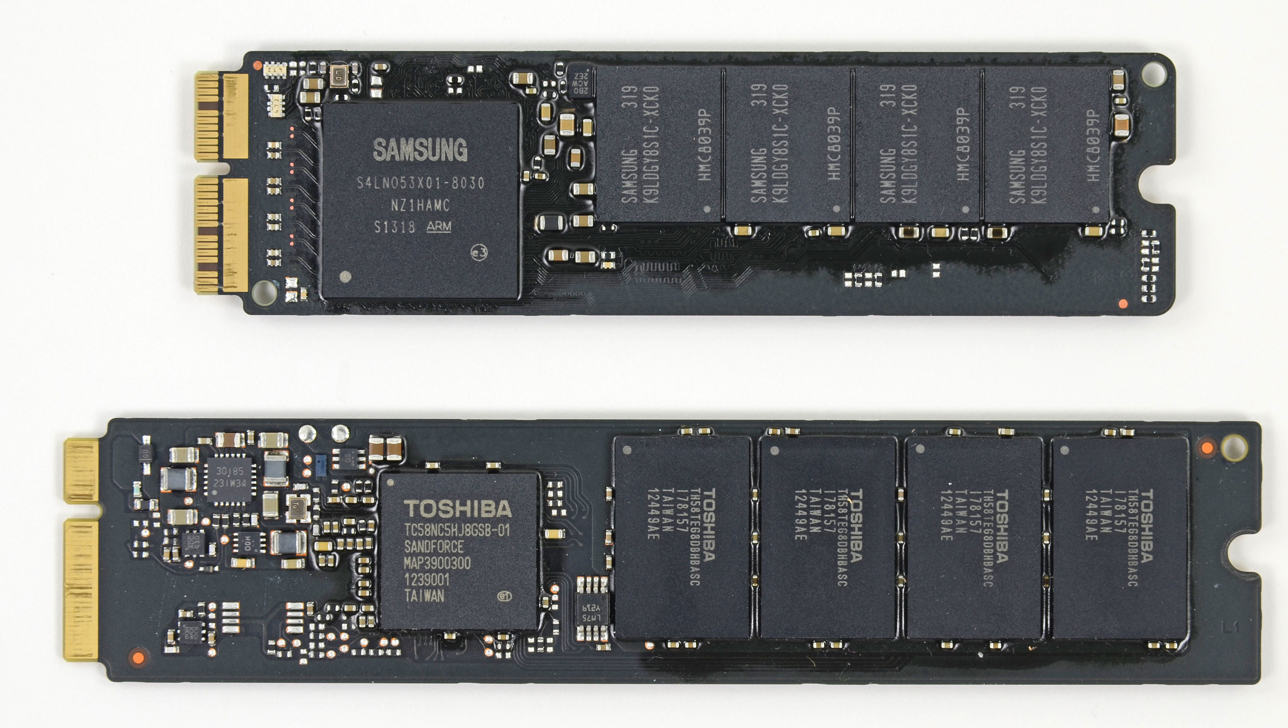
New PCIe SSD (top) vs. 2012 MBA SATA SSD (bottom) - Courtesy iFixit
Despite moving to PCIe, Apple continues to use its own proprietary form factor and interface for the SSD. This isn’t an M.2 drive. The M.2 spec wasn’t far enough along in time for Apple to use it this generation unfortunately. The overall drive is smaller than the previous design, partially enabled by Samsung’s smaller NAND packages.


233 Comments
View All Comments
seapeople - Tuesday, June 25, 2013 - link
Brightness is pretty much the number one power consumer in a laptop like this (which is actually mentioned in the review). If you expect to run anything at 100% brightness and get anywhere near ideal battery life then you are bound to be disappointed.name99 - Monday, June 24, 2013 - link
"802.11ac ... better spatial efficiency within those channels (256QAM vs. 64QAM in 802.11n). Today, that means a doubling of channel bandwidth and a 4x increase in data encoded on a carrier"This is a deeply flawed statement in two ways.
(a) The modulation form describes (essentially) how many bits can be packed into a single up/down segment of a sinusoid wave form, ie how many bits/Hz. It is constrained by the amount of noise in the channel (ie the signal to noise ratio) which smeers different amplitudes together so that you can't tell them apart.
It can be improved somewhat over 802.11n performance by using a better error correcting code (which essentially distributes the random noise level over a number of bits, so that a single large amount of noise rather than destroying that bit information gets spread into a smaller amount of noise over multiple bits).
802.11ac uses LDPC, a better error correcting code, which allows it to use more aggressive modulation.
Point is, in all this the improved modulation has nothing to do with spatial encoding and spatial efficiency.
(b) The QAM64 and QAM256 refer to the number of possible states encoded per bit, not in any way to the number of bits encoded. So QAM64 encodes 6 bits per Hz, QAM256 encodes 8 bits per Hz. the improvement is 8/6=1.33 which is nice, but is not "a 4x increase in data encoded on a carrier".
We are close to the end of the line with fancy modulation. From now on out, pretty much all the heavy lifting comes from
(1) wider spectrum (see the 80 and 160MHz of 802.11ac) and
(2) smaller, more densely distributed base stations.
We could move from 3 up to 4 spatial streams (perhaps using polarization to help out) but that's tough to push further without much larger antennas (and a rapidly growing computational budget).
There is one BIG space for a one-time 2x improvement, namely tossing the 802.11 distributed MAC, which wastes half the time waiting randomly for one party or another to talk, and switching to a centrally controlled MAC (like the telcos) along with a very narrow RACH (random access channel) for lightweight tasks like paging and joining.
My guess/hope is that the successor to 802.11ac will consist primarily of the two issues I've described above (and so will look a lot more like new SW than new DSP algorithms), namely a central arbiter for a network along with the idea that, from the start, the network will consist of multiple small low-power cells working together, about one per room, rather than a single base station trying to reach out to 100 yards or more.
bittwiddler - Monday, June 24, 2013 - link
• The keyboard key size and spacing is the same on the 11 and 13" MBAs.• The 11" MBA is exempt from being removed from luggage during TSA screenings, unlike the 13.
• The 11" screen is lower height than most and doesn't get caught by the clip for the airplane seat tray table.
• When it comes to business travel computing, I'm not interested in a race to the bottom.
Sabresiberian - Monday, June 24, 2013 - link
One thing I would NOT like is for Apple to make a move to a 16:9 screen. I'd certainly rather have 1440x900 on a 13" screen than anything denser that was 16:9. I mean, I'm one of the guys that has been harping on pixel density and refresh rates since before we had modern smart phones (the move to LCDs set us back a decade or more in that regard), but on a screen smaller than 27", 16:9 is just bad. In my not-so-humble opinion.4:3 is better for something smaller than 17", but I can live with 16:10. :)
Kevin G - Monday, June 24, 2013 - link
Re-reading trough the review I have a question about the display: does it use panel self refresh? I recall Intel hyping up this technology several years ago and the Haswell slides in this review indicate support for it. The question is, does Apple take advantage of it?Kevin G - Monday, June 24, 2013 - link
I think that I can answer my own question. I couldn't find the data sheet for the review panel LSN133BT01A02 but references on the web point towards an early 2012 release for it. Thus it looks like it appeared on the market before panel self refresh was slated for wide spread introduction alongside Haswell.hobagman - Monday, June 24, 2013 - link
Hi Anand & all -- could I ask a more CPU related question I've been wondering about a lot -- how come the die shots always look so colorful and diverse, when isn't the top layer all just interconnects? Or are the die shots actually taken before they do the interconnects, consisting in the top 10-15 layers? Would really appreciate an explanation of this ...hobagman - Monday, June 24, 2013 - link
I mean, what are we actually seeing when we look at the die shot? Are those all different transistor regions, and if so, we must be looking at the bottom layers. Or is it that the interconnects in the different regions look different ... or ... ?SkylerSaleh - Tuesday, June 25, 2013 - link
When making the ASIC, thin layers of glass are grown on the silicon, etched, and filled with metal to build the interconnects. This leaves small sharp geometric shapes in the glass, which reacts with the light similarly to how a prism would, causing the wafer to appear colorful.cbrownx88 - Monday, June 24, 2013 - link
Please please please revisit with the i7 config - been wanting to make a purchase but have been waiting for this review (and now waiting on the update lol).