The Haswell Ultrabook Review: Core i7-4500U Tested
by Anand Lal Shimpi on June 9, 2013 9:00 AM ESTHaswell ULT: Platform Power Improvements
Over the past several years, Intel’s maniacal focus on reducing CPU power almost entirely ignored the rest of the platform. Even its own chipsets were often on high power process nodes (remember the first Atom’s 2.5W TDP, but with a 6W chipset TDP). This all changes with Haswell, at least with the ULT/ULX flavors.
I already went through the chipset/PCH changes. The move to 32nm and bringing the PCH on-package will help with power tremendously. But with Haswell, Intel looked beyond its own silicon to other controllers on the motherboard for opportunistic power savings.
With Haswell, Intel deploys its new platform power management framework called Power Optimizer. Its goal? To deliver S3 (suspend to RAM) style power savings, at S0 (active) style latency.
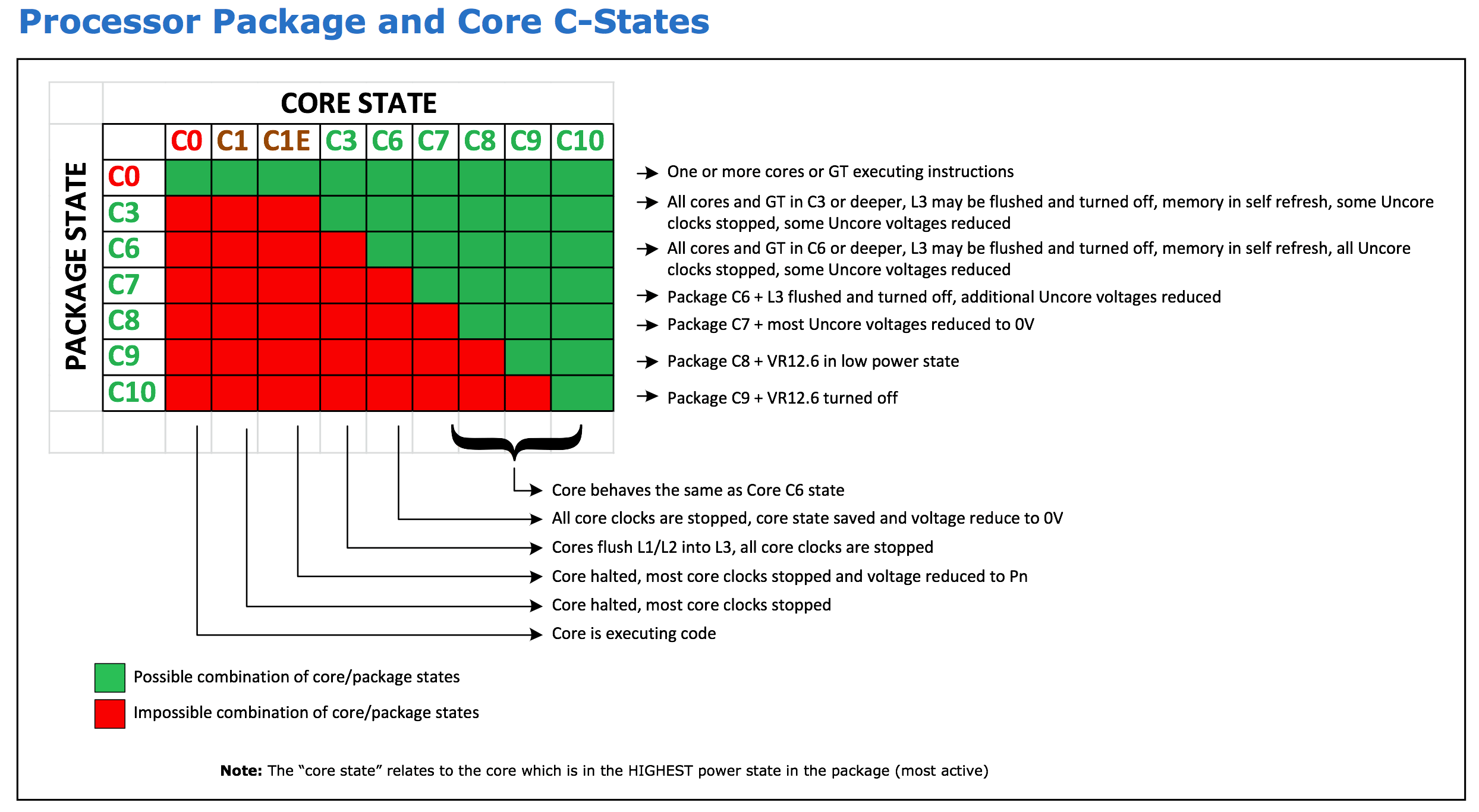
On the CPU, Intel had to dramatically increase its ability to turn blocks on/off, as well as quickly enter/exit its own low power states. Haswell’s FIVR (Fully Integrated Voltage Regular) helps tremendously in this regard as it can quickly switch between voltage states (Intel claims 5x - 10x faster than off-package VR). Haswell as a result can more aggressively choose to go down to lower power states because it can come out of them very quickly. Haswell ULT/ULX support lower core and package C-states. The entire SoC can now be power gated in C10, where the rail that feeds FIVR can be shut off.
For the rest of the platform though, Intel did what the PC industry is best known for: designing a spec and asking others to implement it.
PCIe, SATA, USB 3, DisplayPort are all touched by Power Optimizer. Devices on these busses can report latency tolerance to the PCH (how long can I sleep without breaking everything), and based on that information the PCH can determine how frequently everything has to wake up to avoid impacting user experience.
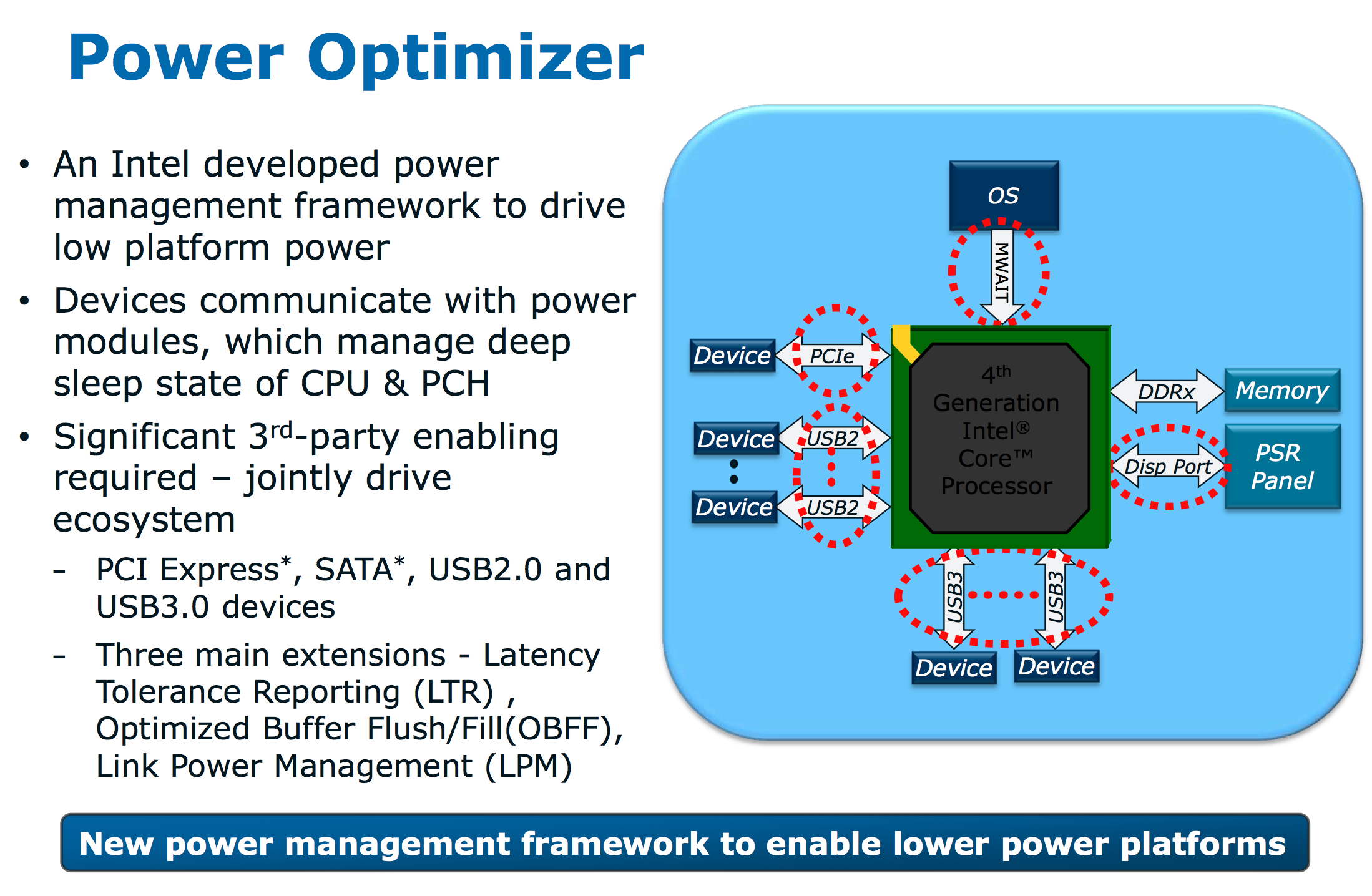
Haswell will take all of the latency tolerance information into account and coordinate system wide sleep/wake based on the least common denominator. The idea is that during idle periods, there’s no reason that most of the platform components can’t be driven down to their lowest power states as if your notebook lid was shut; especially as long as they can quickly wake up when needed. Intel calls this platform level active idle state S0ix, and it’s only supported on Haswell ULT/ULX. In the past Intel had referred to multiple S0ix states, but it looks like Intel is trying to move away from that nomenclature. Effectively now there’s just S0 and S0ix in terms of active power states.
Obviously all it takes is a single 3rd party component to ruin everything, so Intel has worked with device and microcontroller manufacturers to help improve their power profiles as well. Intel’s Power Optimizer architecture is very robust. Intel plans on working with platform vendors regularly to improve power. There are no more easy power gains; going forward, reducing power is going to require a much more collaborative effort from all the power consumers on the platform.
Windows 8 also plays a significant role in all of this as the OS supports coalescing of tasks in software to ensure that it isn’t working against Intel’s Power Optimizer in hardware.
If the CPU/SoC and much of the motherboard can aggressively drive down to S3-like idle power, the display becomes an even bigger burden than it has in the past. To allow the entire platform to go to sleep while the display is still active, Intel recommends Panel Self Refresh (PSR) to be implemented in Haswell Ultrabooks. The idea behind PSR is to put DRAM on the panel itself to store the frame buffer. In the event of a static display (e.g. staring at a Word document, looking at your desktop), the GPU frame buffer is copied to the panel’s DRAM, and the GPU itself is shut off instead of having to drive meaningless content updates to the display 60 times per second. With PSR, the SoC can go into its deepest sleep state (C10).
No Connected Standby for Now
Although you should be able to realize some of the benefits from S0ix with the first Haswell Ultrabooks, Connected Standby (periodic content refresh while in a sleep state) requires OS support. For Haswell Ultrabooks, that means waiting for Windows 8.1.
Even on the S0ix side, it’s not clear to me whether all of the devices in the system capable of going into D3 (their lowest power state) while active will actually do so until Windows 8.1. I get the distinct impression that Haswell Ultrabooks will see a tangible increase in battery life with Windows 8.1.


87 Comments
View All Comments
Rogatti - Sunday, June 9, 2013 - link
GPU Intel.........no thanks !!!!!Kaveri ... where is you !!! ... do not let me down !
A5 - Sunday, June 9, 2013 - link
Anything based on Steamroller isn't going to be able to touch these battery life numbers.If you don't care about battery life, you can get much better value for your money outside of the ultrabook form factor.
Samus - Sunday, June 9, 2013 - link
The GPU performance is slowly creeping up to AMD; AMD won't be able to use their GPU as a crutch much longer.Death666Angel - Sunday, June 9, 2013 - link
Just the ridiculously lower price.kyuu - Monday, June 10, 2013 - link
Yeah, because AMD isn't going to be improving their iGPU tech at all...?nunomoreira10 - Monday, June 10, 2013 - link
not really, intel currently uses an abnormal 180mm2 of die area on 22nm (hd5000) for the same perfomance and efficiency of an 80mm2 28nm amd gpu.the are trying to go all out, but their gpu tech basically sucks
smartypnt4 - Monday, June 10, 2013 - link
Where'd you see the analysis of how much space HD5000 takes? I haven't seen anything on that. Maybe I just missed it...180mm2 of die area for Haswell ULT total is what's been reported, and AMD's Trinity 4C at 28nm is 246mm2. The number of transistors in each is basically identical. The difference comes in where Intel and AMD spend transistors. I'd wager that AMD spends more transistors in GPU, and Intel spends more in CPU.
To be frank, I don't see how you can assert that Intel's <90mm2 of graphics on an integrated chip has appreciably lower efficiency than any other mobile part on the market. I could be wrong, but I just don't see it as that far off.
smartypnt4 - Monday, June 10, 2013 - link
Never mind. Found Anand's analysis. There's no way that's correct though. If 1/2 of GT3 takes up 87mm2, then full GT3 takes up 174mm2. Haswell 2C ULT is a 184mm2 die. There's no way the GPU takes up 90% of the chip. Over half, sure. but 90% is ridiculously high. Something in the 75-80% range is the absolute highest I'd expect.Homeles - Sunday, June 9, 2013 - link
A bit disappointed to see the CPU performance largely stand pat compared to Ivy bridge, but it nailed the one major thing that mattered: battery life.GPU performance isn't awfully inspiring either. I suppose that I won't see the performance gains I was hoping for until Broadwell.
Oh well. I suppose Fall IDF isn't too far away.
meacupla - Sunday, June 9, 2013 - link
Well, i7-4500U is clocked 100mhz slower, but haswell IPC is about 10% better, so obviously CPU performance is not going to differ by much.GPU performance for HD5000 is pretty much what was expected from early intel slides. Iris pro is what was touted as performing up to 'more than 2x' performance.