The Haswell Ultrabook Review: Core i7-4500U Tested
by Anand Lal Shimpi on June 9, 2013 9:00 AM ESTOn-Package PCH, The First Single Chip Haswell
In 2010, with Clarkdale and Arrandale, Intel went from a 3-chip platform solution (CPU, IOH/MCH, ICH) down to a 2-chip platform (CPU + PCH). With Haswell, we see the first instantiation of a single-chip Core platform.
With the 8-series chipset, Intel moved from a 65nm process on the 7-series chipset to 32nm, skipping 45nm entirely. An older, less mobile-focused Intel would try to keep its chipsets on the oldest, economically sensible node possible, but these days things are different. The move to 32nm cuts TDP down considerably. Intel hasn’t publicly documented the power consumption any of its ultra mobile chipsets, but if we look at QM77 to QM87 we see a 34% decrease in TDP.
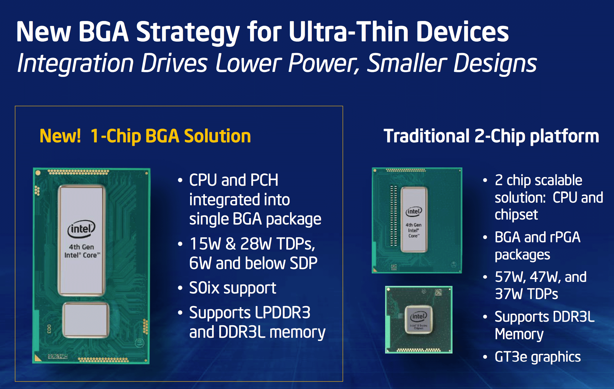
In Haswell desktop and standard voltage mobile parts, the 8-series chipset remains a an off-chip solution in a discrete package. With Haswell ULT and ULX (U and Y series SKUs), the 8-series PCH (Platform Controller Hub) moves on-package. Since it’s on-package, the TDP of the PCH is included in the overall TDP of the processor.
Bringing the PCH on-package not only saves space on the motherboard, but it also reduces the power needed to communicate with the chip. Signals no longer have to travel off die, through the package, via traces on the motherboard to the PCH. Instead you get much lower power on-package communication.
Intel also changed the interface between the CPU and PCH to a new on-package interface instead of DMI. Presumably Intel’s OPI is designed for much lower power operation.
Although PCIe support remains on the PCH (6 PCIe 2.0 lanes), there’s no external PCIe interface from the CPU itself. Any hopes for pairing a meaningfully high performance discrete GPU with Haswell ULT are dead. We didn’t see a ton of Ivy Bridge Ultrabooks with discrete GPUs, but the option simply won’t exist this time around. All of the sudden the creation of Intel’s 28W Haswell ULT with GT3 graphics makes a lot more sense. Haswell ULT lacks native VGA support. Update: NVIDIA tells me that it fully supports running a dGPU off of a x4 connection to the PCH. It's not the ideal solution, but discrete GPUs will still technically be possible with Haswell ULT.
Intel adds SDIO support. USB 3 and 6Gbps SATA are both there as well (although with fewer max ports supported compared to the desktop PCH, up to 4 and 3 respectively). There’s also a lot more sharing of bandwidth between individual PCIe lanes and USB/SATA. These limits shouldn’t be an issue given the port/drive configuration of most Ultrabooks.


87 Comments
View All Comments
Rogatti - Sunday, June 9, 2013 - link
GPU Intel.........no thanks !!!!!Kaveri ... where is you !!! ... do not let me down !
A5 - Sunday, June 9, 2013 - link
Anything based on Steamroller isn't going to be able to touch these battery life numbers.If you don't care about battery life, you can get much better value for your money outside of the ultrabook form factor.
Samus - Sunday, June 9, 2013 - link
The GPU performance is slowly creeping up to AMD; AMD won't be able to use their GPU as a crutch much longer.Death666Angel - Sunday, June 9, 2013 - link
Just the ridiculously lower price.kyuu - Monday, June 10, 2013 - link
Yeah, because AMD isn't going to be improving their iGPU tech at all...?nunomoreira10 - Monday, June 10, 2013 - link
not really, intel currently uses an abnormal 180mm2 of die area on 22nm (hd5000) for the same perfomance and efficiency of an 80mm2 28nm amd gpu.the are trying to go all out, but their gpu tech basically sucks
smartypnt4 - Monday, June 10, 2013 - link
Where'd you see the analysis of how much space HD5000 takes? I haven't seen anything on that. Maybe I just missed it...180mm2 of die area for Haswell ULT total is what's been reported, and AMD's Trinity 4C at 28nm is 246mm2. The number of transistors in each is basically identical. The difference comes in where Intel and AMD spend transistors. I'd wager that AMD spends more transistors in GPU, and Intel spends more in CPU.
To be frank, I don't see how you can assert that Intel's <90mm2 of graphics on an integrated chip has appreciably lower efficiency than any other mobile part on the market. I could be wrong, but I just don't see it as that far off.
smartypnt4 - Monday, June 10, 2013 - link
Never mind. Found Anand's analysis. There's no way that's correct though. If 1/2 of GT3 takes up 87mm2, then full GT3 takes up 174mm2. Haswell 2C ULT is a 184mm2 die. There's no way the GPU takes up 90% of the chip. Over half, sure. but 90% is ridiculously high. Something in the 75-80% range is the absolute highest I'd expect.Homeles - Sunday, June 9, 2013 - link
A bit disappointed to see the CPU performance largely stand pat compared to Ivy bridge, but it nailed the one major thing that mattered: battery life.GPU performance isn't awfully inspiring either. I suppose that I won't see the performance gains I was hoping for until Broadwell.
Oh well. I suppose Fall IDF isn't too far away.
meacupla - Sunday, June 9, 2013 - link
Well, i7-4500U is clocked 100mhz slower, but haswell IPC is about 10% better, so obviously CPU performance is not going to differ by much.GPU performance for HD5000 is pretty much what was expected from early intel slides. Iris pro is what was touted as performing up to 'more than 2x' performance.